The AMD Vega GPU Architecture Teaser: Higher IPC, Tiling, & More, Coming in H1’2017
by Ryan Smith on January 5, 2017 9:00 AM ESTFirst Thoughts: A Peek At What’s To Come
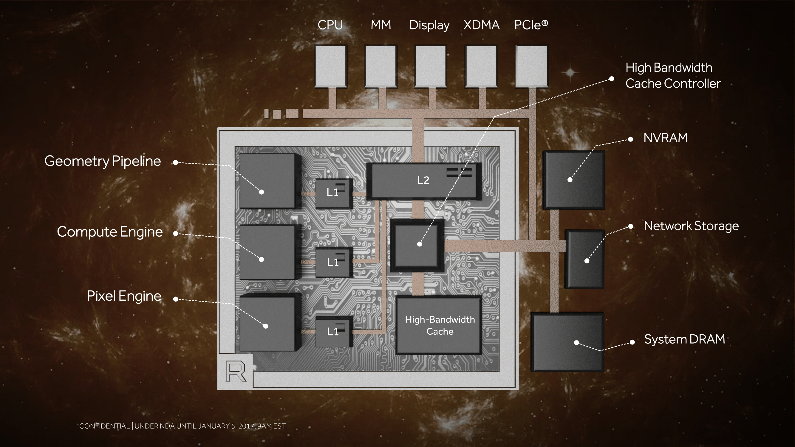
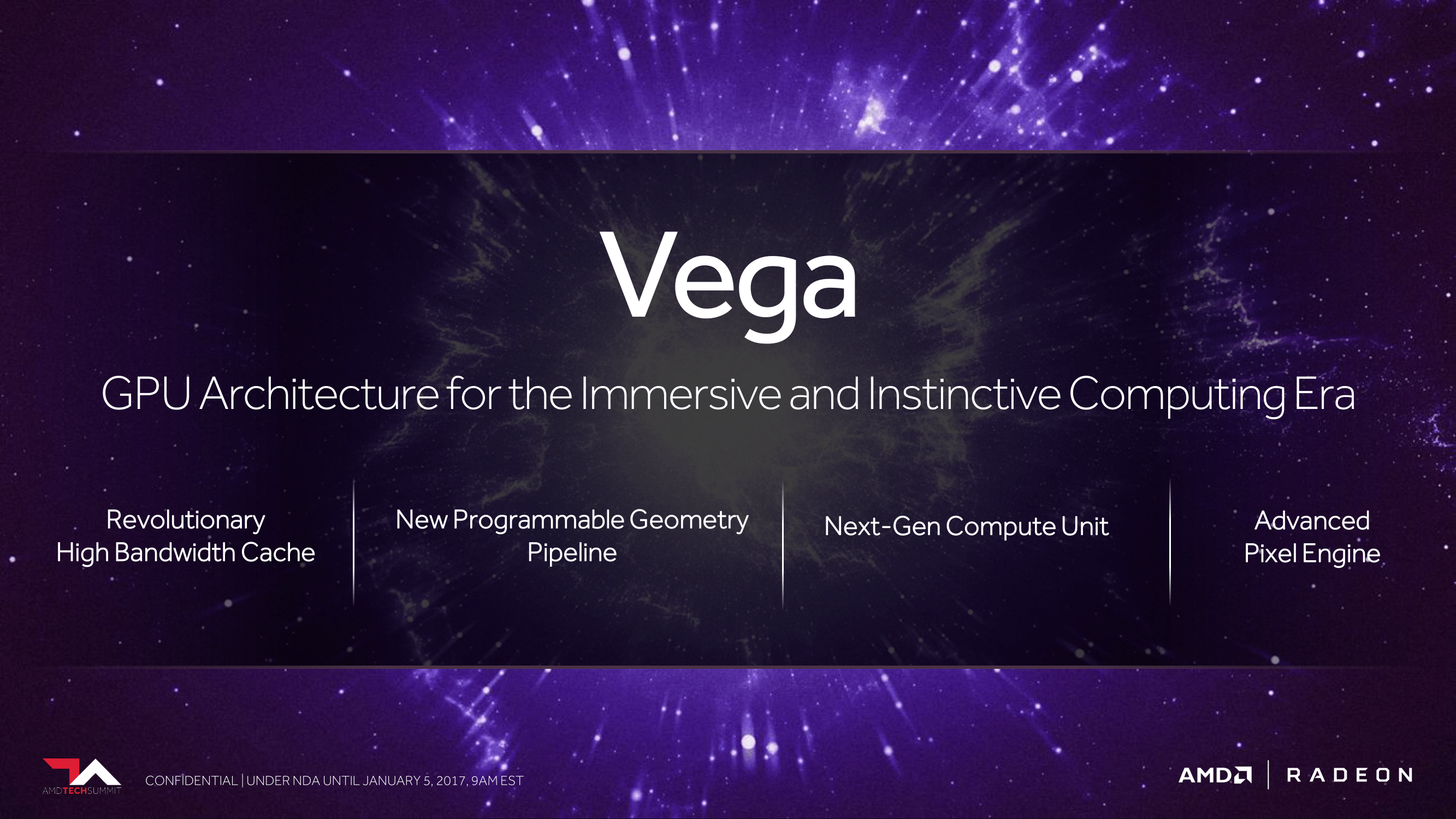
Wrapping things up, while today’s reveal from AMD is only a teaser of what they have been working on over the last few years with Vega, it’s none the less an important one. Based on what we know so far, Vega stands to be the biggest change to AMD’s GPU architecture since GCN 1.0 was released 5 years ago, and the changes to the ALUs, the ROPs, the memory structure, and other aspects of Vega reinforce this notion. To be sure, Vega is not a wholly new architecture – it is clearly a further refinement of GCN – but then this is exactly why GCN was designed to be able to evolve through refinements over a very long period of time.
What we have for now then is a quick look at what’s to come from AMD. There are still many things we don’t know, not the least of which is the actual GPU configurations. But for a teaser it’s enough to show that AMD has been hard at work. It sets the stage for the hardware and marketing ramp-up to come over the next few months.
But for now, let’s close with an image. As I mentioned before, the first Vega has taped out, and Radeon Technology Group’s frontman and Chief Architect, Raja Koduri, has one. The chip was just a few weeks old as of December, and while trying to discern die size may be a little too error-prone, we can see one important detail: 2 HBM2 packages.

Raja and AMD will not tell us what chip we’re looking at – like Polaris, two Vega chips have been confirmed – but either way we are looking at one of them in all its alpha silicon glory. Bearing in mind HBM2’s much greater bandwidth per pin, we could very well be looking at a design for a Fiji-like 512GB/sec of memory bandwidth in the chip Raja holds. And for AMD, that is one more teaser for today to keep attention focused right where they want it: on Vega ahead of its H1’17 launch.


155 Comments
View All Comments
eldakka - Friday, January 6, 2017 - link
Don't use URL obfuscation services. They are a major security risk, as they can hide malware attack vectors as you don't know the true final destination of the URL. For all I know that tinyurl could be going to a malicious site that tries to load malware into your browser.Never click on an obfuscated URL, that's as basic as never opening an email attachment from an unknown source.
Threska - Saturday, January 7, 2017 - link
That's why it has a preview function built in were you can see where it goes first before continuing on.Threska - Saturday, January 7, 2017 - link
I should add that the only practical resolution to the twin problems, too-long URLs and the issues they cause and who do you trust, is Anandtech running their own URL-shortening service.tuxRoller - Saturday, January 7, 2017 - link
Ha!I ALWAYS forget to use those services:)
versesuvius - Friday, January 6, 2017 - link
It has become sickening to listen to AMD years in advance about what they are going to do for the next eon, which is nothing but talking anyway. Wise to stop reading about anything GPU until Intel buys NVIDIA out and gets it all sorted out and done with.lobz - Friday, January 6, 2017 - link
alright then... just let us know when you're sober againMeteor2 - Saturday, January 7, 2017 - link
It's a fair point and I would not be at all surprised if Intel used its cash to buy Nvidia; Intel is clearly struggling to find the Next Big Thing (5G? Really?); Nvidia is not, with IP ideal for making AI happen.Threska - Sunday, January 8, 2017 - link
Cash isn't the only thing needed for a buyout. Nvidia has to be willing to be bought. An IP exchange would be easier for both companies.Gastec - Friday, January 13, 2017 - link
There are these little nuisances called antitrust laws but with Donald Trump as President of the USA anything is possible :)Alexvrb - Friday, January 6, 2017 - link
The "High Bandwidth Cache" could also be a hint of what's to come with future HBM2-capable APUs. Intel has a cache up to what, 128MB of eDRAM? I think even a single HBM2 stack could provide a huge boost to an APU.