Samsung Foundry Announces 10nm SoC In Mass-Production
by Andrei Frumusanu on October 17, 2016 5:40 AM EST- Posted in
- Semiconductors
- Samsung
- fabrication
- 10LPE
Today Samsung announced mass production of a SoC built on its third-generation 10nm "10LPE" manufacturing node. It was only this January that Samsung announced mass production of its 14LPP process that ended up being used in the Exynos 8890 and the Snapdragon 820 powering up a large amount of flagship devices this year.
This time around the announcement comes quite early compared to the past 2 years and I wasn't expecting any news from the foundry till maybe later in the quarter. This does however bode well for the SoCs built on the process as they seem they'll be able to easily make the spring 2017 device release schedule.
There wasn't any specification as to what kind of SoC the mass production announcement is refering to, but it's very likely we're talking about S.LSI's next generation Exynos - or maybe even Qualcomm's Snapdragon 820 successor, both of which we'll hopefully hear official announcements from in the coming months.
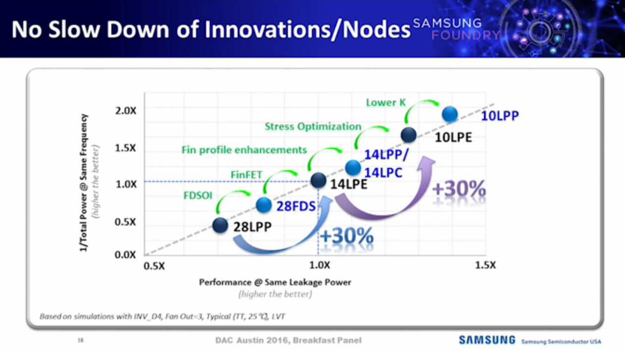
Samsung’s new 10nm FinFET process (10LPE) adopts an advanced 3D transistor structure with additional enhancements in both process technology and design enablement compared to its 14nm predecessor, allowing up to 30-percent increase in area efficiency with 27-percent higher performance or 40-percent lower power consumption. In order to overcome scaling limitations, cutting edge techniques such as triple-patterning to allow bi-directional routing are also used to retain design and routing flexibility from prior nodes.
Credit: DAC 2016 Samsung/Synopsys Breakfast - Ready to Design at 10nm!
The process promises some significant speed and power efficiency advantages over current generation designs so it's likely the next generation of devices will see a large boost, similarly to how the first 14/16 SoCs had large improvements over previous generation 20/28nm designs.
Interestingly the new SoCs will have an edge on recent and upcoming designs still being released on 16nm manufacturing processes, such as Apple's A10 or other TSMC customers who have to wait till next year for 10FF. This presents itself as an opportunity for vendors such as Samsung and Qualcomm to try to close the performance and efficiency gap seen in the current generation through the manufacturing process' good timing.
Source: Press Release


92 Comments
View All Comments
SydneyBlue120d - Monday, October 17, 2016 - link
I wonder who will use the new process other than Samsung itself and Qualcomm?fanofanand - Monday, October 17, 2016 - link
For years we have been pining for AMD to step up their game to give Intel some competition, but it looks like it will be Samsung instead. AMD might still push them hard with Zen but Intel is suddenly awash in competition where it previously had none. I don't think now is a good time to be long in Intel stock.looncraz - Monday, October 17, 2016 - link
AMD is partnered with Samsung and GloFo for production.AMD has stated they are jumping to 7nm GloFo, though, so it's unclear if they will use Samsung's 10nm or if GloFo will license it.
fanofanand - Monday, October 17, 2016 - link
AMD is partnering with TSMC and has to pay GloFo for each chip produced at TSMC. The agreement itself is very interesting. GloFo will license Sammy's 10 nm tech, I think the side agreement with TSMC was for Vega, and to put a spur in GloFo's behind to get them working harder to catch up.iwod - Monday, October 17, 2016 - link
Triple Patterning in Samsung 10nm??!!! Wow, that means Samsung is ahead of the game? If i remember TSMC only goes to Triple Pattering in 7nm.And this means it is likely to be the first time in the last two decade Intel has lost in leading edge Fab tech for real ( Not node numbering ). Although Intel 10nm should be out sometimes in 2017 too.
vladx - Monday, October 17, 2016 - link
It's not that others can't use triple patterning it's just that it's very expensive and Samsung can afford it with very few risks.witeken - Tuesday, October 18, 2016 - link
You are unfortunately incorrect.First, you are incorrect that Intel hasn't lost its manufacturing lead in two decades. The most recent time was at 28nm, which launched in AMD GPUs in January 2012, which is in fact denser than Intel's 32nm, which was only followed by their 22nm in April.
Second, triple patterning does not mean anything. The only thing it means is that Samsung's 10nm will be significantly costlier to manufacture than Intel's 14nm.
So here's a fun fact: Samsung's SRAM cell size is only 1.2x bigger than Intel's 14nm SRAM size which is made with double patterning.
So Samsung's "10nm" will only be modestly denser than Intel's 14nm. Intel's 10nm will be about 1.6x denser than Samsung's 10nm.
So there you go.
The_Assimilator - Monday, October 17, 2016 - link
All these people saying Intel is behind make me laugh. There's a reason they're nicknamed Chipzilla.fanofanand - Monday, October 17, 2016 - link
The reason is that they were (for the better part of history) the leading edge fabricator of semiconductors. That is changing, and changing rapidly. Anyone saying Intel's lead has not diminished makes ME laugh. If you don't think there is panic at Intel over the recent blunders you are crazy. Mobile was a dead-end where they wasted BILLIONS, IBM and ARM are elbowing in on the server space, AMD has a compelling server chip coming, and now Samsung is eating away at their foundry leads. Chipzilla is crashing down to earth very quickly, and I suspect their margins will come down with it.Michael Bay - Tuesday, October 18, 2016 - link
>Mobile was a dead-end where they wasted BILLIONSTheir billions to waste, not mine. Experience in lowpower is what they got out of it.
>IBM and ARM are elbowing in on the server space
In their dreams they surely do.
>AMD has a compelling server chip coming
We hear that for how many years exactly now?
>Samsung is eating away
Until it starts exploding. Or touting 14nm as 10.