Samsung Foundry Announces 10nm SoC In Mass-Production
by Andrei Frumusanu on October 17, 2016 5:40 AM EST- Posted in
- Semiconductors
- Samsung
- fabrication
- 10LPE
Today Samsung announced mass production of a SoC built on its third-generation 10nm "10LPE" manufacturing node. It was only this January that Samsung announced mass production of its 14LPP process that ended up being used in the Exynos 8890 and the Snapdragon 820 powering up a large amount of flagship devices this year.
This time around the announcement comes quite early compared to the past 2 years and I wasn't expecting any news from the foundry till maybe later in the quarter. This does however bode well for the SoCs built on the process as they seem they'll be able to easily make the spring 2017 device release schedule.
There wasn't any specification as to what kind of SoC the mass production announcement is refering to, but it's very likely we're talking about S.LSI's next generation Exynos - or maybe even Qualcomm's Snapdragon 820 successor, both of which we'll hopefully hear official announcements from in the coming months.
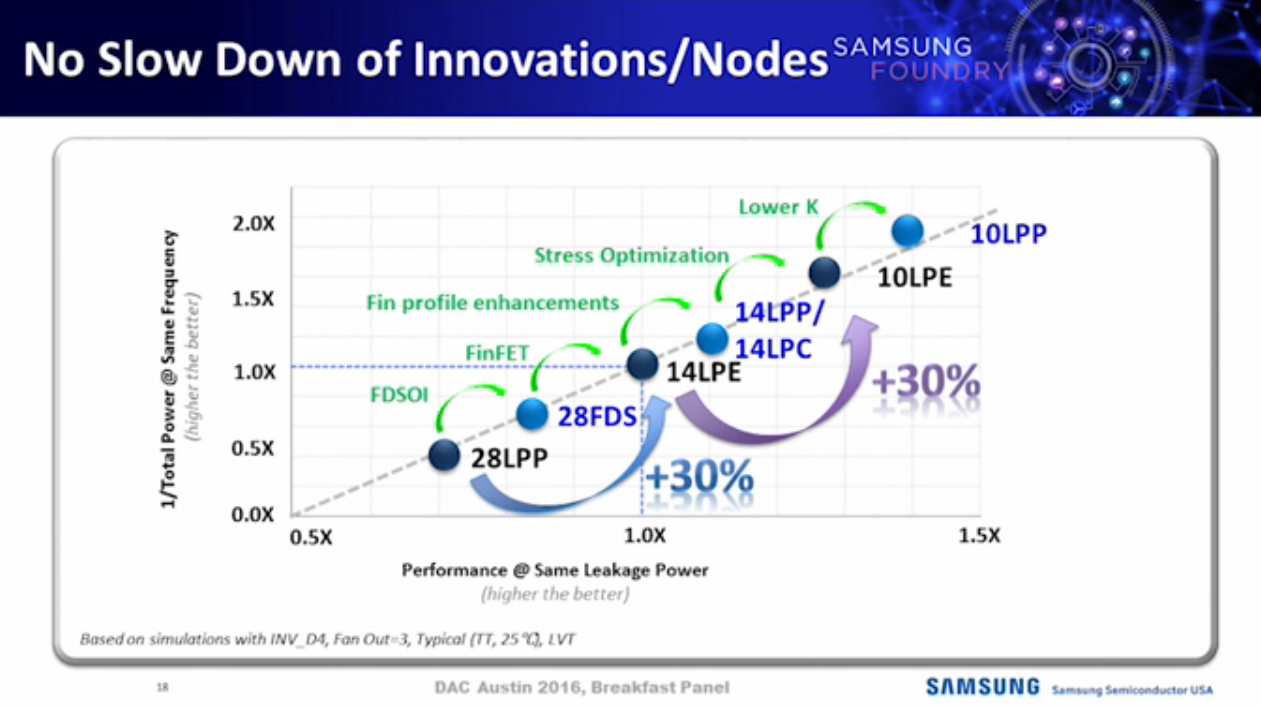
Samsung’s new 10nm FinFET process (10LPE) adopts an advanced 3D transistor structure with additional enhancements in both process technology and design enablement compared to its 14nm predecessor, allowing up to 30-percent increase in area efficiency with 27-percent higher performance or 40-percent lower power consumption. In order to overcome scaling limitations, cutting edge techniques such as triple-patterning to allow bi-directional routing are also used to retain design and routing flexibility from prior nodes.
Credit: DAC 2016 Samsung/Synopsys Breakfast - Ready to Design at 10nm!
The process promises some significant speed and power efficiency advantages over current generation designs so it's likely the next generation of devices will see a large boost, similarly to how the first 14/16 SoCs had large improvements over previous generation 20/28nm designs.
Interestingly the new SoCs will have an edge on recent and upcoming designs still being released on 16nm manufacturing processes, such as Apple's A10 or other TSMC customers who have to wait till next year for 10FF. This presents itself as an opportunity for vendors such as Samsung and Qualcomm to try to close the performance and efficiency gap seen in the current generation through the manufacturing process' good timing.
Source: Press Release


92 Comments
View All Comments
fanofanand - Monday, October 17, 2016 - link
As much as I enjoy being correct (and let me tell you, I do enjoy it) I am wrong on this one. " The phrase "xx nm node" means that the smallest spacing between repeated features on a chip along one direction is xx nm. It does not actually mean that transistors are now xx nm by xx nm. "So it's not the feature size it's the minimum distance between features. Of course that does make your statement "there is nothing that measures 14 nm" incorrect as well.
Source: http://nanoscale.blogspot.com/2015/07/what-do-ibms...
p1esk - Monday, October 17, 2016 - link
As your source article shows, the "node size" is supposed to be the channel length. I think this is still somewhat true for Intel.witeken - Tuesday, October 18, 2016 - link
No, node name has nothing to do with channel length or any other length.Intel 22nm channel length was 28nm. Their 14nm channel length is 20nm, their 90nm channel length was about 45nm.
witeken - Tuesday, October 18, 2016 - link
Incorrect. I don't care what your cute blog says, it is wrong. Go to WikiChip and look at the feature sizes. Feature size are not a secret, at least not all of them :). So please come back if you found something to be 10nm or whatever ;).witeken - Tuesday, October 18, 2016 - link
Unfortunately, your memory is incorrect. You can search the literature all you want, but I can promise you that you will never find even a single feature to be the length of the node name for ANY node in the past 15 years, let alone any node in the future. It's marketing. TSMC and Samsung 14/16nm have same density as their 20nm, for instance.ViRGE - Monday, October 17, 2016 - link
That's true for any process though. No process comes online ready to fab massive chips with a reasonable yield.lefty2 - Monday, October 17, 2016 - link
I don't know about that. TSMC seem to start straight away with big die SoCs. The A10X is ment to be the first 10nm part.Also, consider that Intel won't start manufacturing high end CPUs on 10nm until 2018. That's more than a year with poor yields and why they had to introduce a new CPU family, coffee lake.
extide - Monday, October 17, 2016 - link
Yeah but A10X is going to be probably a 150mm^2 part MAX -- that's not a big die part. Polaris 10 is about 300mm^2 or so, GP100 is over 600mm^2, and Intel's Knight's Landing is 683mm^2 -- those are big dies, especially the latter two.psychobriggsy - Tuesday, October 18, 2016 - link
Well, whilst Polaris 10 is 223mm^2 (not 300), GF's 14nm Foundry Yields are extremely good (0.08 defects per cm^2).Another factor is routing - TSMC and GF 14/16 allow 2D routing, which is denser than the 1D routing that Intel use. So whilst Intel's transistors have the capability of being closer together and denser, in practice that cannot happen a lot of the time.
And after that, another factor is how many metal layers can be made on the finest BEOL scale (20nm for TSMC/GF, 14nm for Intel). Intel IIRC can do 4 1D layers at this scale. GF IIRC can do 8 2D layers for a GPU-oriented design targeting density.
So as you can see there are so many variable that arguing about the process name is difficult. They all have pros and cons. Intel's biggest Pro was being the first to market by over a year, but that's fading away right now. They still have per-transistor power usage (although TSMC seem to compete looking at Pascal GPUs).
witeken - Tuesday, October 18, 2016 - link
In theory (based on transistor area), Intel's 14nm node is 1.4x denser than Samsung's 2D 14nm node. In practice, it is indeed about 1.4x denser. So the 2D routing's impact is negligible.