Samsung Foundry Announces 10nm SoC In Mass-Production
by Andrei Frumusanu on October 17, 2016 5:40 AM EST- Posted in
- Semiconductors
- Samsung
- fabrication
- 10LPE
Today Samsung announced mass production of a SoC built on its third-generation 10nm "10LPE" manufacturing node. It was only this January that Samsung announced mass production of its 14LPP process that ended up being used in the Exynos 8890 and the Snapdragon 820 powering up a large amount of flagship devices this year.
This time around the announcement comes quite early compared to the past 2 years and I wasn't expecting any news from the foundry till maybe later in the quarter. This does however bode well for the SoCs built on the process as they seem they'll be able to easily make the spring 2017 device release schedule.
There wasn't any specification as to what kind of SoC the mass production announcement is refering to, but it's very likely we're talking about S.LSI's next generation Exynos - or maybe even Qualcomm's Snapdragon 820 successor, both of which we'll hopefully hear official announcements from in the coming months.
Samsung’s new 10nm FinFET process (10LPE) adopts an advanced 3D transistor structure with additional enhancements in both process technology and design enablement compared to its 14nm predecessor, allowing up to 30-percent increase in area efficiency with 27-percent higher performance or 40-percent lower power consumption. In order to overcome scaling limitations, cutting edge techniques such as triple-patterning to allow bi-directional routing are also used to retain design and routing flexibility from prior nodes.
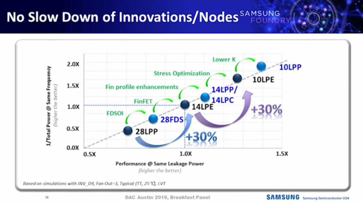
Credit: DAC 2016 Samsung/Synopsys Breakfast - Ready to Design at 10nm!
The process promises some significant speed and power efficiency advantages over current generation designs so it's likely the next generation of devices will see a large boost, similarly to how the first 14/16 SoCs had large improvements over previous generation 20/28nm designs.
Interestingly the new SoCs will have an edge on recent and upcoming designs still being released on 16nm manufacturing processes, such as Apple's A10 or other TSMC customers who have to wait till next year for 10FF. This presents itself as an opportunity for vendors such as Samsung and Qualcomm to try to close the performance and efficiency gap seen in the current generation through the manufacturing process' good timing.
Source: Press Release


92 Comments
View All Comments
sseemaku - Tuesday, October 18, 2016 - link
Seems like everybody got bought into the marketing. Historically, each process node brought 50% scaling or double the transistor count in given area. But no foundry is following this anymore. In samsung's case, the scaling is 30% but called 10nm. Good marketing.witeken - Tuesday, October 18, 2016 - link
Correct, although even the 50% is not usually reached. It varies a lot from node to nodes. In the last nodes however, at 14nm and 10nm and likely again at 7nm, Intel has indeed shrunk or will shrink by about 2x density. For comparison, TSMC has already said their 7nm will shrink by 1.63x.