OpenCAPI Unveiled: AMD, IBM, Google, Xilinx, Micron and Mellanox Join Forces in the Heterogenous Computing Era
by Johan De Gelas on October 14, 2016 8:00 AM EST- Posted in
- CPUs
- Enterprise

Some of you may remember AMD announcing the "Torrenza" technology 10 years ago. The idea was to offer a fast and coherent interface between the CPU and various types of "accelerators" (via Hyper Transport). It was one of the first initiatives to enable "heterogeneous computing".
We now have technology that could be labeled "heterogeneous computing", the most popular form being GPU computing. There have been also encryption, compression and network accelerators, but the advantages of those accelerators were never really clear, as shifting data back and forth to the CPU was in many cases less efficient than letting the CPU process it with optimized instructions. Heterogeneous computing was in the professional world mostly limited to HPC; in the consumer world a "nice to have".
But times are changing. The sensors of the Internet of Things, the semantic web and the good old www are creating a massive and exponentially growing flood of data that can not be stored and analyzed by traditional means. Machine learning offers a way of classifying all that data and finding patterns "automatically". As a result, we witnessed a "machine learning renaissance", with quite a few breakthroughs. Google had to deal with this years ago before most other companies, and released some of those AI breakthroughs of the Google Brain Team in the Open Source world, one example being "TensorFlow". And when Google releases important technology into the Open Source world, we know we got to pay attention. When Google released the Google File System and Big Table back in 2004 for example, a little bit later the big data revolution with Hadoop, HDFS and NoSQL databases erupted.
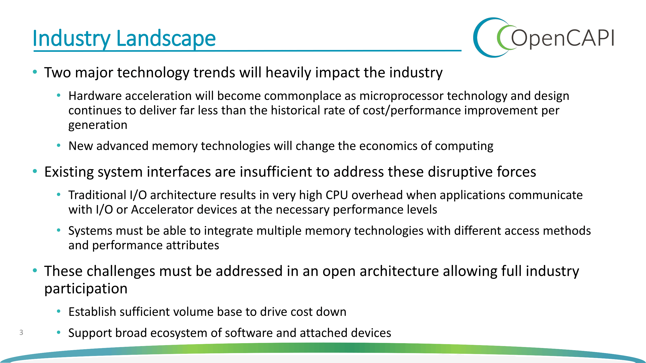
Big Data thus needs big brains: we need more processing power than ever. As Moore's law is dead (the end of CMOS scaling), we can not expect much from process technology advancements. The processing power has to come from ASICs (see Google's TPU), FPGAs (see Microsoft's project Catapult) and GPUs.
Those accelerators need a new "Torrenza technology", a fast, coherent interconnect to the CPU. NVIDIA was first with NVLink, but an open standard would be even better. IBM on the other hand was willing to share the CAPI interface.
To that end, Google, AMD, Xilinx, Micron and Mellanox have joined forces with IBM to create a "coherent high performance bus interface" based on a new bus standard called "Open Coherent Accelerator Processor Interface" (OpenCAPI). Capable of a 25Gbits per second per lane data rate, OpenCAPI outperforms the current PCIe specification, which offers a maximum data transfer rate of 8Gbits per second for a PCIe 3.0 lane. We assume that the total bandwidth will be a lot higher for quite a few OpenCAPI devices, as OpenCAPI lanes will be bundled together.
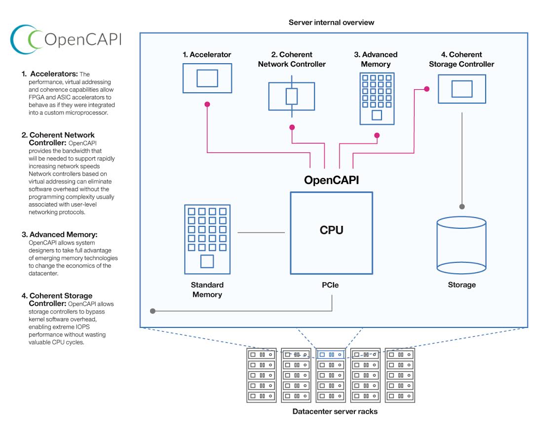
It is a win, win for everybody besides Intel. It is clear now that IBM's OpenPOWER initiative is gaining a lot of traction and that IBM is deadly serious about offering an alternative to the Intel dominated datacenter. IBM will implement the OpenCAPI interface in the POWER9 servers in 2017. Those POWER9s will not only have a very fast interface to NVIDIA GPUs (via NVLink), but also to Google's ASICs and Xilinx FPGAs accelerators.
Meanwhile this benefits AMD as they get access to an NVLink alternative to link up the Radeon GPU power to the upcoming Zen based server processors. Micron can link faster (and more profitable than DRAM) memory to the CPU. Mellanox can do the same for networking. OpenCAPI is even more important for the Xilinx FPGAs as a coherent interface can make FPGAs attractive for a much wider range of applications than today.
And guess what, Dell/EMC has joined this new alliance just a few days ago. Intel has to come up with an answer...
Update: courtesy of commenter Yojimbo: "NVIDIA is a member of the OpenCAPI consortium, at the "contributor level", which is the same level Xilinx has. The same is true for HPE (HP Enterprise)".
This is even bigger than we thought. Probably the biggest announcement in the server market this year.


Source: OpenCAPI


49 Comments
View All Comments
wyewye - Saturday, October 15, 2016 - link
I second that. We really dont need your multiple pages of idiotic "philosophy" Johan. This entire article is only "25Gbits per second per lane". The rest is complete garbage.tuxRoller - Sunday, October 16, 2016 - link
It's actually 16-112GT/s/lane, and you can aggregate up to 256 lanes. That's a lot faster.It's also not even close to the whole story.
tuxRoller - Sunday, October 16, 2016 - link
Ugh. Ignore. Wrong article.Meteor2 - Wednesday, December 21, 2016 - link
Would you talk to your mother like that? Be more civil.Johan is completely correct with his analysis and you'd do well to listen if you don't want to be behind the times.
fanofanand - Friday, October 14, 2016 - link
Forgive my ignorance, but isn't Pci-E 4.0 supposed to double the bandwidth to 32Gbits/s? If that's the case, what good is this new interconnect? Can it supply more power than a traditional Pci-E lane? I just don't understand the "why" behind this.diehardmacfan - Friday, October 14, 2016 - link
PCI-E 4.0 is 32Gbit/s with 16 lanes, this is 25GB/sec with 1 lane.LoneRat - Friday, October 14, 2016 - link
Its 25Gbit/s, not GByte/s.BTW this interface is almost obsolete since it doesn't offer anything superior than PCI-E 3.0. It is more like a "half-node" between PCI-E 3.0 16Gbps and 4.0 32Gbps. Intel may just need to push 4.0 out earlier to battle it. Since PCI-E 4.0 is backward compatible with 3.0 while OCAPI is a completely new interface (and I doubt it will be compatible with PCIE standard), OCAPI won't be as popular as PCIE.
By the way, OCAPI might become a competing standard to PCIE, but implementing 2 different standards on to 1 die of a SoC will be ridiculous. Unless IBM can find a way to emulate/support PCIE on OCAPI or unless OCAPI is a more efficient route, the new interface will be dead like IBM's other non-standard, non-compatible interfaces in the old days.
close - Friday, October 14, 2016 - link
This isn't just another interface for your gaming card.PCIe 3.0 offers 8Gbps and PCIe 4.0 doubles that to 16Gbps over one lane versus the 25Gbps for Open CAPI. Add the full coherency to that and you get something that addresses exactly the issues the industry has right now with the available interconnects.
You're right, it won't be very popular among the guys looking to get a GeForce GTX2080 for their PC...
fatpenguin - Friday, October 14, 2016 - link
This isn't accurate - PCIe 3.0 offers 8GT/sec per lane (Gen 2 is effectively 4GT/sec after the 8b/10b). PCIe 4 is supposed to offer 16GT/sec per lane. With 16 lanes, it's 32GB/sec.Also, this is 25Gbit/sec, not 25GB/sec. 16 lanes would give 50GB/sec of bandwidth.
I don't understand where the article's claims of 16Gbit/sec per lane for PCIe 3.0 come from. That's where PCIe 4.0 comes in.
Either way, this is considerably faster per lane, and likely offers less overhead / latency than PCIe, which is where the majority of performance improvements lie...PCIe has quite a bit of overhead for small transactions.
What about mechanical changes? I'd be a bit surprised if they are trying to achieve this rate with the same constraints (edge card connector, etc).
rhysiam - Friday, October 14, 2016 - link
That data rate for PCIe 3.0 made me pause too. It's bidirectional, so my guess is that Johan was quoting it as (almost) 8Gb per second, per lane, per direction, so 16Gb total bandwidth (counting send and receive).