Early iPhone 7 Teardowns: Intel & Qualcomm Modems, TSMC SoC, 2 to 3 GB of RAM
by Ryan Smith on September 16, 2016 10:15 AM EST- Posted in
- Smartphones
- Mobile
- iPhone 7
- iPhone 7 Plus
- Chipworks
- iFixit
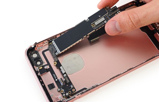
Today is launch date for Apple’s new iPhone 7 models, and as is tradition every year, the teardowns have already begun. Both the Chipworks/TechInsights team and iFixit have completed their respective initial teardowns of the iPhone 7 and 7 Plus, tearing part some of the first phones to go on sale. These teardowns are preliminary – there’s a lot of work left to do in deciphering the many cryptic identification numbers of the various components – but right off the bat it confirms a few things about each of the phones.
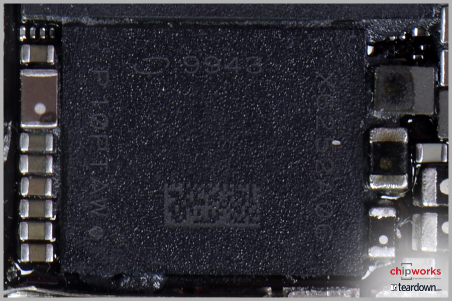
We’ll start off with the Chipworks teardown of an iPhone 7, which they have already earnestly begun identifying chips on. One of their immediate findings is that for the first time in a while, Apple is using a non-Qualcomm modem. On Chipworks’ GSM phone, they have found an Intel baseband processor with the model number PMB9943. They believe this to be part of Intel’s XMM 7360 modem, which was announced back in 2015.

The XMM 7360 is a high-end LTE Advanced modem design that offers up to Category 10 performance (450 Mbps down). This is achieved in part through the use of 3x carrier aggregation, which allows the modem to use up to 60Mhz of wireless spectrum. The modem does not support CDMA, and as the iFixit team has turned up a Qualcomm Snapdragon X12 (Cat 12) modem in their unit, Apple is clearly using modems from multiple vendors. It’s not clear how this breakdown works – if Apple is using the Qualcomm modem in some GSM phones as well – but at a minimum the Qualcomm modem will have to be in all of the CDMA-capable models.
Meanwhile for Intel’s modem group, this is a significant win, as the company has not seen too many high-profile device wins in recent years. Though historically speaking, this is actually something of a return to form. The original iPhone used a modem from the group’s predecessor, Infineon’s wireless unit, whom Intel purchased in 2010.
Moving on, we have of course the A10 Fusion SoC. Chipworks has yet to get a die shot in, but they have already confirmed that the SoC is produced by TSMC. This is presumably another 16nm FinFET SoC, but the Chipworks team will be working to confirm that. So far there is no evidence to indicate that Apple is dual-sourcing SoCs on the iPhone 7 like they did the iPhone 6s, but this is again preliminary information.

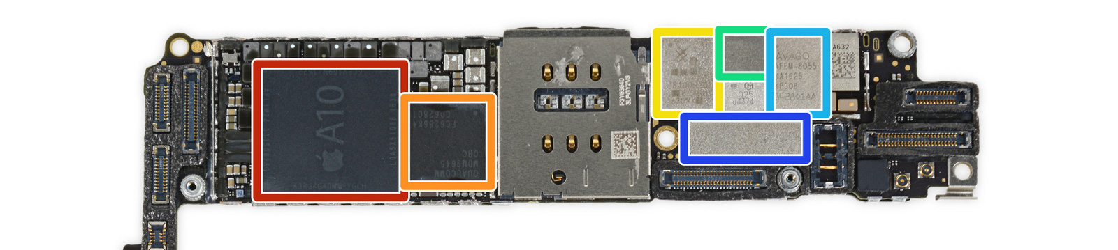
Given that Apple doesn’t get a major new manufacturing process to use this generation, I had been wondering if and how Apple would instead compromise on die size, and we now have a rough answer. Chipworks estimates the A10 die to be roughly 125mm2 in size. This is 20.5mm2 (~20%) larger than the A9 TSMC die. The good news for Apple is that yields should be much better in 2016 than they were in 2015, so chip manufacturing costs should be down, helping to offset the higher costs of the larger chip. And while there are ways to improve performance without increasing the die size, any kind of significant improvement would have to entail a larger die, which is exactly what we’re seeing here. If nothing else, Apple would need more room for the new high-efficiency CPU cores the chip packs in.
Speaking of packing, Chipworks’ teardown also hints that the A10 may have been packaged using TSMC’s new Integrated Fan Out (InFO) technique, which is meant to allow for thinner chip packages. InFO saves space, in part, by eliminating the organic substrate that logic dies have traditionally been mounted on.

Lastly with the A10, Chipworks’ teardown of their iPhone 7 confirms that it has 2GB of RAM, specifically Samsung LPDDR4. Besides confirming that the memory capacity on the iPhone 7 hasn’t increased versus the iPhone 6s, this is notable because iFixit has found something different with their iPhone 7 Plus. In the case of the larger phone, there is 3GB of RAM. Apple has never before equipped the Plus with more memory than the base model, so this is a first. And while there has always been some performance stratification between the two phones due to the Plus model’s larger size – allowing better heat dissipation, and therefore slightly better performance – I wonder if this means we’re going to see an increase in the stratification between the two phone models. If nothing else, I suspect this comes as a consequence of the Plus’s higher resolution screen: all other factors being held equal, the Plus needs a bit more RAM for its larger GPU frame buffers.
Update: The Chipworks crew has their die shot and floor plan back, so let's take a look.
![]()
As Apple already disclosed the number of GPU clusters, there's not a whole lot left to doubt in terms of basic construction.The GPU cores, SRAM caches, and the performance CPU cores are all easy enough to find, with the latter block now about 16mm2, versus 13mm2 in the A9. The big question here is where the two smaller, high-efficiency cores are. Chipworks postulates three thories: 1) They're in the same block as the high performance cores (and hence labeled as a quad core CPU), they're to the left of the die, or they're to the bottom left of the die.
It is likely - but not guaranteed - that they're close to the high-performance cores. However both alternative locations do have pairs of identical blocks, which is what you'd be looking for in a secondary set of CPU cores. So although those options are less likely, without additional information it's difficult to rule out those options entirely.
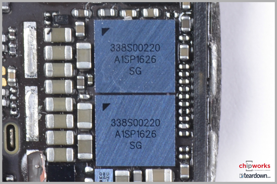
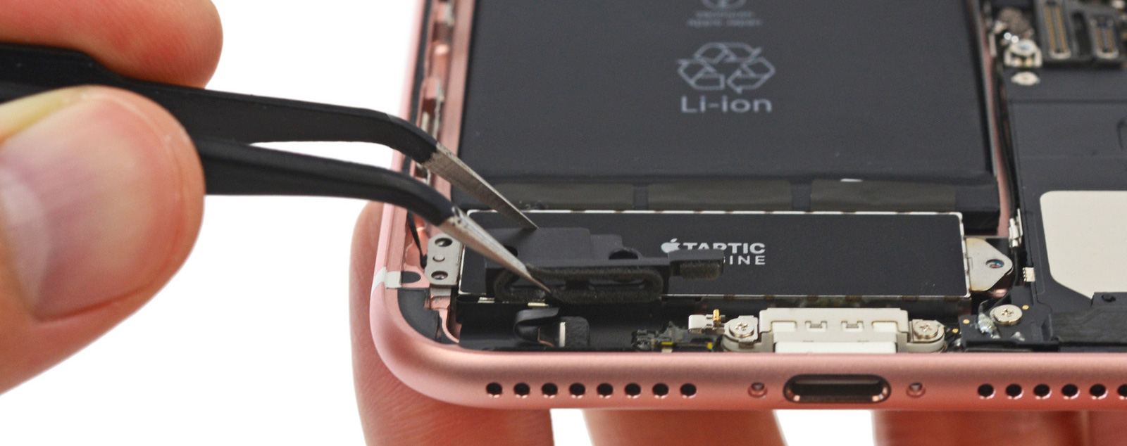
Finally, one interesting aspect of the Chipworks report is that they unexpectedly found a third audio amplifier. Chipworks was expecting to find two – one for each of the speakers – but came up with a third. The firm believes that the third amp may be for headphones, which in turn would mean that Apple has significantly revised the Lightning port specification for the iPhone 7. Previously Lightning has only carried digital audio, which doesn’t require an amp in the phone itself. In the initial iPhone 7 announcement I had speculated that Apple put the DAC (and amp) inside their 3.5mm adapter – which would be consistent with how Lightning has worked over the last 4 years – but this casts doubt on that idea. If Apple has revised the specification to allow analog audio over the port, then this greatly simplifies how headphones and adapters will work. But it also would raise a number of questions about peripheral compatibility, especially what happens if you plug something like the Lightning EarPods into an older device like the iPhone 5s.
On that note, the Chipworks and iFixit teardowns also show us what’s gone in the place of the now-absent headphone jack: Apple has placed a taptic engine (linear actuator) for the solid state home button, and an unusual plastic bumper.
Wrapping things up, Chipworks’ reports that they already have the A10 SoC in their lab for further work, including confirming the manufacturing process and, of course, a die shot. The latter should prove to be very interesting, as it will be the first look we get at Apple’s new high-efficiency CPU cores. And in the meantime on our end we also have our iPhone samples in-house, so we’re diligently working on putting together a review for later this month. So be sure to stay tuned for that.


96 Comments
View All Comments
solipsism - Monday, September 19, 2016 - link
It's weird that both iFixit and AnandTech would report it as a near useless piece of plastic used as a bumper for the haptic motor when it clearly has a cable connecting it to the board and a water-resistant seal around it when it sit over the holes in the casing.lefty2 - Saturday, September 17, 2016 - link
> Until you can find a carrier to give you 450 mbps download speeds I'm not sure it really matters.You're right. The download speed probably doesn't matter too much. What does matter is the Qualcomm modem is much better than Intel's. Better signal reception and lower power consumption. Also, I believe the X12 is 20nm, while Intel's modem is on 28nm.
mrvco - Sunday, September 18, 2016 - link
As homogenized as the smart phone market has become, I'm surprised anyone still bothers with these teardowns.kfishy - Monday, September 19, 2016 - link
Regarding where the smaller cores are, it looks like it may be sandwiched in between the two SRAM blocks. The L1 and L2 caches look quite small, but since it's so close to L3 and clocked so low it may not make a difference.Vulpy - Saturday, September 24, 2016 - link
Looking at the iPhone 7 HW, I can't stop thinking of Nokia s last yrs as a phone manufacturer.They played it so safe (I was an engineer in the mobile comm business working with them and Samsung at that time), and they thought innovation is an outdated concept, believing that people look for absolute performance e as opposed to new ideas, design and customization.
Apple is heading that way too, give them 2 yrs and they will be history.
lowtolerance - Monday, September 26, 2016 - link
LOL that is nothing but magical thinking. Apple has enough cash on reserve that they could operate as they do today and still last way longer than two years even if they never sold another device.