AMD Zen Microarchiture Part 2: Extracting Instruction-Level Parallelism
by Ian Cutress on August 23, 2016 8:45 PM EST- Posted in
- CPUs
- AMD
- x86
- Zen
- Microarchitecture
Some Final Thoughts and Comparisons
With the Hot Chips presentation we’ve been given more information on the Zen core microarchitecture than we expected to have at this point in the Zen design/launch cycle. AMD has already stated that general availability for Zen will be in Q1, and Zen might not be the final product launch name/brand when it comes to market. However, there are still plenty of gaps in our knowledge for the hardware, and AMD has promised to reveal this information as we get closer to launch.
We discussed in our earlier piece on the Zen performance metrics given mid-week that it can be hard to interpret any anecdotal benchmark data at this point when there is so much we don’t know (or can’t confirm). With the data in this talk at Hot Chips, we can fill out a lot of information for a direct comparison chart to AMD’s last product and Intel’s current offerings.
| CPU uArch Comparison | ||||
| AMD | Intel | |||
| Zen 8C/16T 2017 |
Bulldozer 4M / 8T 2010 |
Skylake 4C / 8T 2015 |
Broadwell 8C / 16T 2014 |
|
| L1-I Size | 64KB/core | 64KB/module | 32KB/core | 32KB/core |
| L1-I Assoc | 4-way | 2-way | 8-way | 8-way |
| L1-D Size | 32KB/core | 16KB/thread | 32KB/core | 32KB/core |
| L1-D Assoc | 8-way | 4-way | 8-way | 8-way |
| L2 Size | 512KB/core | 1MB/thread | 256KB/core | 256KB/core |
| L2 Assoc | 8-way | 16-way | 4-way | 8-way |
| L3 Size | 2MB/core | 1MB/thread | >2MB/cire | 1.5-3MB/core |
| L3 Assoc | 16-way | 64-way | 16-way | 16/20-way |
| L3 Type | Victim | Victim | Write-back | Write-back |
| L0 ITLB Entry | 8 | - | - | - |
| L0 ITLB Assoc | ? | - | - | - |
| L1 ITLB Entry | 64 | 72 | 128 | 128 |
| L1 ITLB Assoc | ? | Full | 8-way | 4-way |
| L2 ITLB Entry | 512 | 512 | 1536 | 1536 |
| L2 ITLB Assoc | ? | 4-way | 12-way | 4-way |
| L1 DTLB Entry | 64 | 32 | 64 | 64 |
| L1 DTLB Assoc | ? | Full | 4-way | 4-way |
| L2 DTLB Entry | 1536 | 1024 | - | - |
| L2 DTLB Assoc | ? | 8-way | - | - |
| Decode | 4 uops/cycle | 4 Mops/cycle | 5 uops/cycle | 4 uops/cycle |
| uOp Cache Size | ? | - | 1536 | 1536 |
| uOp Cache Assoc | ? | - | 8-way | 8-way |
| uOp Queue Size | ? | - | 128 | 64 |
| Dispatch / cycle | 6 uops/cycle | 4 Mops/cycle | 6 uops/cycle | 4 uops/cycle |
| INT Registers | 168 | 160 | 180 | 168 |
| FP Registers | 160 | 96 | 168 | 168 |
| Retire Queue | 192 | 128 | 224 | 192 |
| Retire Rate | 8/cycle | 4/cycle | 8/cycle | 4/cycle |
| Load Queue | 72 | 40 | 72 | 72 |
| Store Queue | 44 | 24 | 56 | 42 |
| ALU | 4 | 2 | 4 | 4 |
| AGU | 2 | 2 | 2+2 | 2+2 |
| FMAC | 2x128-bit | 2x128-bit 2x MMX 128-bit |
2x256-bit | 2x256-bit |
Bulldozer uses AMD-coined macro-ops, or Mops, which are internal fixed length instructions and can account for 3 smaller ops. These AMD Mops are different to Intel's 'macro-ops', which are variable length and different to Intel's 'micro-ops', which are simpler and fixed-length.
Excavator has a number of improvements over Bulldozer, such as a larger L1-D cache and a 768-entry L1 BTB size, however we were never given a full run-down of the core in a similar fashion and no high-end desktop version of Excavator will be made.
This isn’t an exhaustive list of all features (thanks to CPU World, Real World Tech and WikiChip for filling in some blanks) by any means, and doesn’t paint the whole story. For example, on the power side of the equation, AMD is stating that it has the ability to clock gate parts of the core and CCX that are not required to save power, and the L3 runs on its own clock domain shared across the cores. Or the latency to run certain operations, which is critical for workflow if a MUL operation takes 3, 4 or 5 cycles to complete. We have been told that the FPU load is two cycles quicker, which is something. The latency in the caches is also going to feature heavily in performance, and all we are told at this point is that L2 and L3 are lower latency than previous designs.
A number of these features we’ve already seen on Intel x86 CPUs, such as move elimination to reduce power, or the micro-op cache. The micro-op cache is a piece of the puzzle we want to know more about, especially the rate at which we get cache hits for a given workload. Also, the use of new instructions will adjust a number of workloads that rely on them. Some users will lament the lack of true single-instruction AVX-2 support, however I suspect AMD would argue that the die area cost might be excessive at this time. That’s not to say AMD won’t support it in the future – we were told quite clearly that there were a number of features originally listed internally for Zen which didn’t make it, either due to time constraints or a lack of transistors.
We are told that AMD has a clear internal roadmap for CPU microarchitecture design over the next few generations. As long as we don’t stay for so long on 14nm similar to what we did at 28/32nm, with IO updates over the coming years, a competitive clock-for-clock product (even to Broadwell) with good efficiency will be a welcome return.


106 Comments
View All Comments
extide - Monday, August 29, 2016 - link
No,k dude, it's not the same 4 ALU's, it's 4 ALU's per core. 2 threads a core, so 2 ALU's/thread, up to 16 threads, or 4 ALU's /thread up to 8 threads, but I would think it would be hard for a single thread to use 4 ALU's, so having 2 threads per 4 ALU seems fine, plus all the INT execution resources.Outlander_04 - Thursday, August 25, 2016 - link
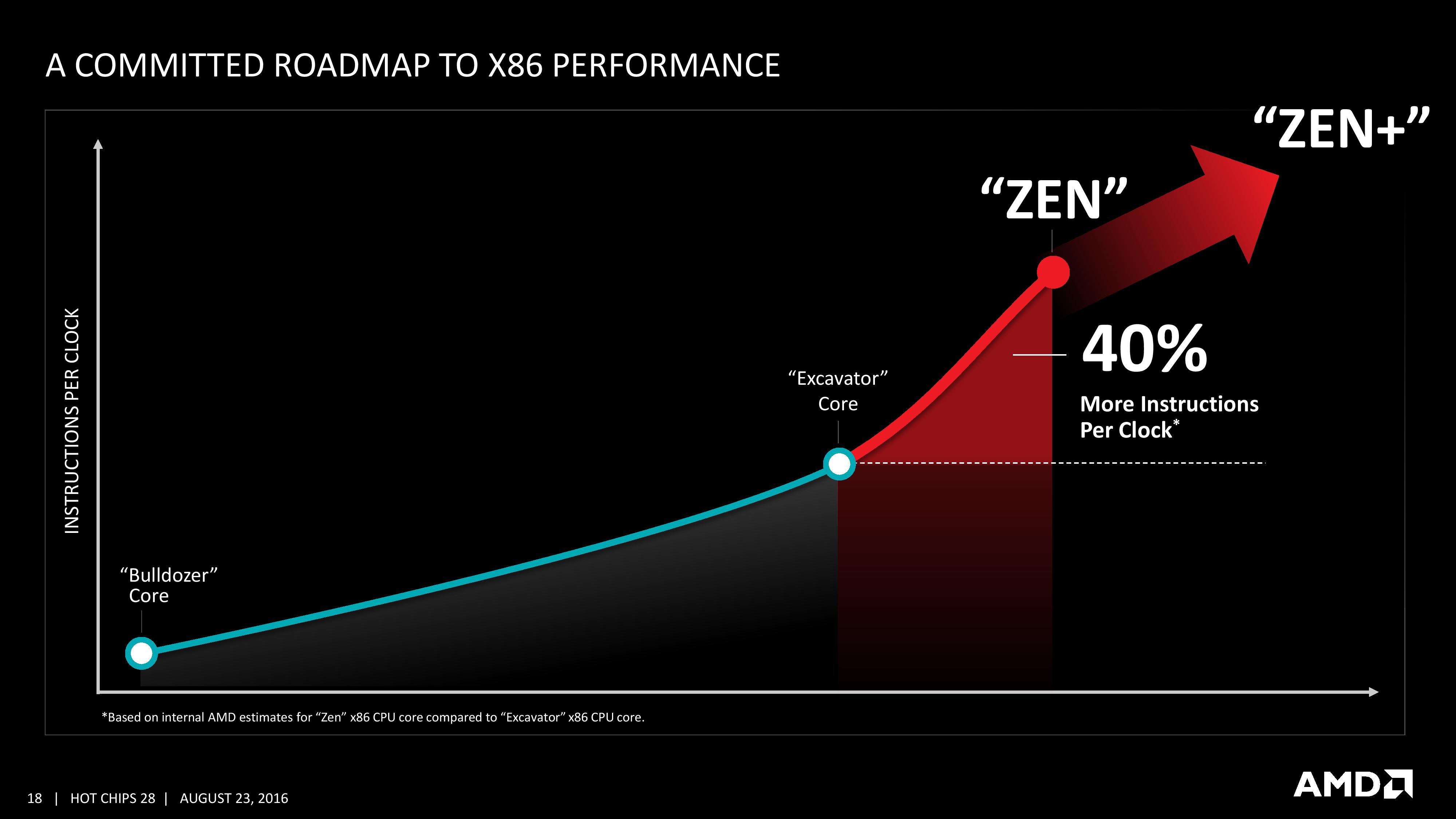
40% improvement is not over Bulldozer but over Excavator which is already 20% or more ahead of Bulldozerlooncraz - Wednesday, August 24, 2016 - link
Highly scalar code or vector code will exceed 40% easily. The core execution resources relative to that execution is 75% to 100% greater. That will only translate to 50~60% performance improvement for said code, but a larger impact than the overall 40% improvement.The cache system, schedulers, issue width, AGUs, L/S, and other factors come more into play in the more common code paths, which reduces the maximum potential benefit derived from the additional execution resources.
However, multi-threaded performance should be HIGHER, not lower. Excavator had relatively poor MT scaling, Zen will be worlds better. Add SMT to the mix - and AMD's solution looks nearly exactly as I anticipated - and you have another 20% or so better SMT scaling.
It is easily conceivable, given what we now know, that AMD has met Haswell's average IPC outside of wider AVX workloads, and exceeded it in certain areas with heavy mixed compute (floating and integer concurrently). It is also now conceivable that AMD's first SMT implementation will be better than Intel's Sandy Bridge era Hyper-Threading. I didn't expect that at all, but the core flexibility is far ahead of Intel's flexibility - and that is largely what determines SMT performance in Zen's design.
Finally, <3Ghz @ 200W is way worse than the currently known figures for their 8C parts. They have 3.2Ghz boost clocks and just 95W TDP. It is expected that the clocks will increase, particularly for the quad core, 65W, parts.
You may not realize this, but these numbers put AMD slightly ahead of Intel in perf/W on 14nm.
niva - Wednesday, August 24, 2016 - link
So are you telling me my Phenom 2 black edition rig might be getting a worthy upgrade?I'm with you, but I don't trust these benchmarks, wait until the retail CPU samples are out then we can decide.
looncraz - Wednesday, August 24, 2016 - link
I'm saying you'll be able to match that level of performance with a Dual core Zen CPU w/ SMT... if AMD were actually to make one (doubtful).I do expect AMD to release triple core CPUs again, though, but possibly not right away.
Myrandex - Thursday, August 25, 2016 - link
Yay finally I've been holding onto my Phenom II as well and this might be it! :)Bulat Ziganshin - Thursday, August 25, 2016 - link
For vector code - they added 4'th ALU, it's almost nothing (Skylake added 4th scalar ALU and got laughable +3% IPC).For scalar code - they advertize +40% IPC. I'm pretty sure that they advertize the best part of perfromance, not the average one. It's ADVERTIZEMENT, after all.
Now, it's easy to analyze Zen as Carrizo+. M/t performance shouldn't change much since it's still 4-wide core (which was called module in Carrizo). S/t performance should improve much more since it changed from 2 alu to 4 alu. Overall, the core looks like Skylake, but it's not enough to put a lot of resources - they need to be carefully placed. Intel gone a long way optimizing their CPUs, and AMD have to repeat that. If you think that AMD can make Skylake-speed CPU in 2 years, then ask yourself - why Intel hasn't done the same in 2008 or so? Why IBM, having WIDER cpu, still slower than Intel in s/t tests?
All we know that AMD was able to SELECT single CPU that was able to run at 3 GHz using cooler looking like one they ship with 95W cpus. Just ask yourself - why they not tried to run their cpu at the same 3.2 GHz which is stock freq. for Intel CPU? And yes, it's way more effificent than Intel CPUs can, making me highly suspicious.
In one of pictures here AMD claims that Zen has the same power usage as Carrizo, that is 28nm CPU. AFAIR Carrizo with 2 modules at ~3GHz use 35-65 Wt. Multiple it by 4, please.
> It is also now conceivable that AMD's first SMT implementation will be better than Intel's Sandy Bridge era Hyper-Threading.
Why?? Intel's first SMT implementation in Pentium4 made a few percents improvement (over s/t), second one in Nehalem give me +20% on deflate, Sandy was +40%, and Haswell is +50%. Why you think that FIRST AMD attempt on SMT will be better than Pentium4?
Overall, i think that m/t perfromance of Zen is more predictable - it's Carrizo with some improvements, but still 4-wide, so i expect usual 10-20% generation-to-generation improvement.
For s/t, it less predictable, but i'm sure that it's impossible to beat Intel in single step, and AMD already advertized +40%, which i'm sure is about s/t perfromance.
looncraz - Thursday, August 25, 2016 - link
"For vector code - they added 4'th ALU, it's almost nothing (Skylake added 4th scalar ALU and got laughable +3% IPC)."Well, that was the average program performance increase, but the vector code itself sped up more than that.
Also, Zen's ability to leverage its resources should be better than Intel's, but its scheduler setup is really unique, so we need more details on how it will handle holes in a scheduler when its neighbor is full. Having six 14-deep schedulers is a significant part of the design that is almost completely overlooked, IMHO.
"Now, it's easy to analyze Zen as Carrizo+. M/t performance shouldn't change much since it's still 4-wide core"
Only if you are comparing a full module to a single Zen core... There were many bottlenecks in the modules that prevented full performance for multi-threading - Zen does not have that. On top, Zen has SMT, so it will have even better MT performance per core.
"Why IBM, having WIDER cpu, still slower than Intel in s/t tests?"
The width is, as you say, only a part of the equation. It's all about being able to exploit that extra width. Intel does so decently well, but has restrictions as a result of their unified scheduler. A heavy FPU load reduces integer performance, for example, due to shared ports of the scheduler. The impact of this is not easily quantifiable - it would require some very specialized testing. Zen will not have this issue thanks to dedicated schedulers.
Intel uses their unified scheduler to be able to provide results more quickly to dependent instructions. Zen, from appearances, allows each scheduler to make fetch and load requests directly, thereby nullifying what used to be an Intel advantage - and maybe even turning it into a hindrance.
"Just ask yourself - why they not tried to run their cpu at the same 3.2 GHz which is stock freq. for Intel CPU?"
Because you don't push engineering sample CPUs, and 3Ghz is the defacto industry standard speed for IPC comparison testing. Just look around, you'll find 3Ghz is the most commonly chosen frequency when doing IPC comparisons on modern CPUs. Pushing both to 3.2Ghz would not have changed anything, but a Zen engineering sample chip is worth thousands more than that Intel CPU at this time, and is not easily replaceable. If you have to run 500 more tests with it, and hand it over to other departments or teams, you probably aren't being allowed to overclock it any.
deltaFx2 - Friday, August 26, 2016 - link
The answer to the IBM question is easy. 1) IBM designed the Power8 with SMT-2 as the sweet spot. Like bulldozer, or Alpha EV6, they have execution clusters. In 2T, each cluster runs a thread, in 1T, the thread is split across these clusters, with a penalty for moving between them. Hence their 1T->2T uplift is a lot higher than intel's 1T->2T (worse baseline). (2) You're comparing different ISAs. x86 is a lot more CISC'y than POWER. x86 supports load+compute, compute+store, load+compute+store, and this is dispatched as a single uop. The same "work" in a more RISC'y machine needs 2 or 3 uops. For the same reason, an ARM core that hopes to achieve the same performance as x86 will need to dispatch more ops, or fuse more ops before dispatch.Spunjji - Saturday, August 27, 2016 - link
The CPU they tasted with is an early engineering sample. Simple answer. You write a lot to make yourself sound smart but you're exercising either clear bias or ignorance here.