AMD Zen Microarchiture Part 2: Extracting Instruction-Level Parallelism
by Ian Cutress on August 23, 2016 8:45 PM EST- Posted in
- CPUs
- AMD
- x86
- Zen
- Microarchitecture
The High-Level Zen Overview
AMD is keen to stress that the Zen project had three main goals: core, cache and power. The power aspect of the design is one that was very aggressive – not in the sense of aiming for a mobile-first design, but efficiency at the higher performance levels was key in order to be competitive again. It is worth noting that AMD did not mention ‘die size’ in any of the three main goals, which is usually a requirement as well. Arguably you can make a massive core design to run at high performance and low latency, but it comes at the expense of die size which makes the cost of such a design from a product standpoint less economical (if AMD had to rely on 500mm2 die designs in consumer at 14nm, they would be priced way too high). Nevertheless, power was the main concern rather than pure performance or function, which have been typical AMD targets in the past. The shifting of the goal posts was part of the process to creating Zen.
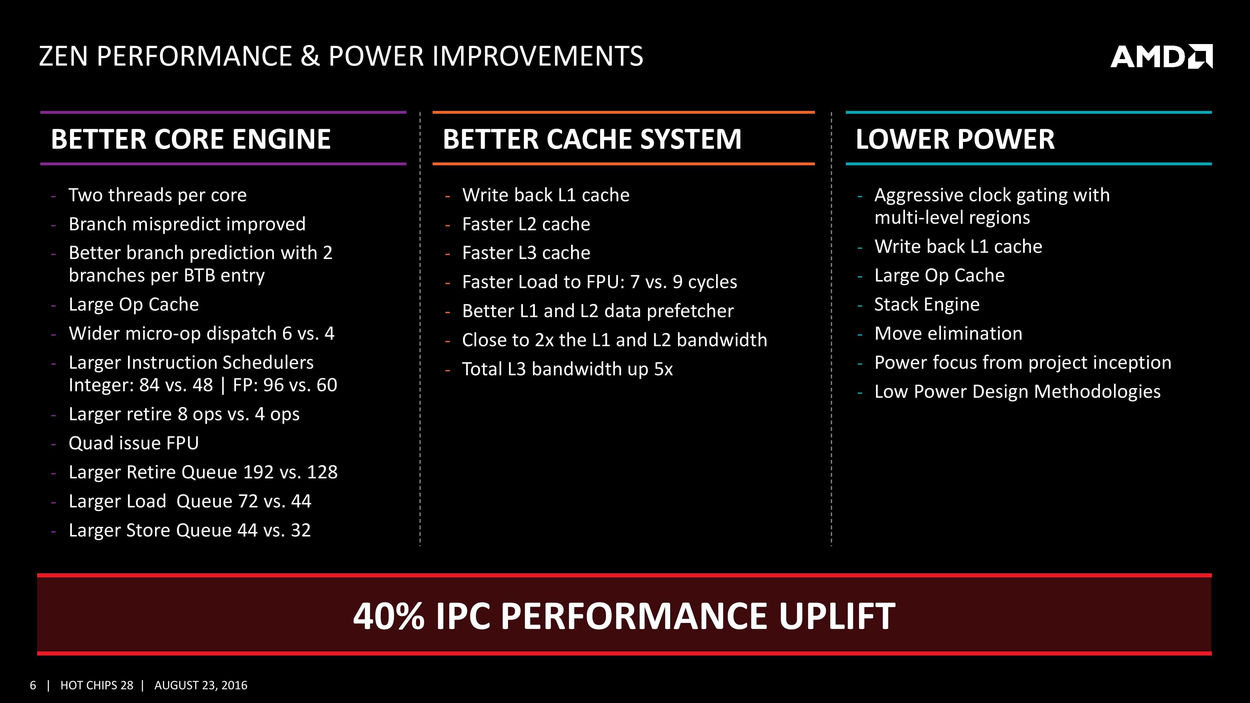
This slide contains a number of features we will hit on later in this piece but covers a number of main topics which come under those main three goals of core, cache and power.
For the core, having bigger and wider everything was to be expected, however maintaining a low latency can be difficult. Features such as the micro-op cache help most instruction streams improve in performance and bypass parts of potentially long-cycle repetitive operations, but also the larger dispatch, larger retire, larger schedulers and better branch prediction means that higher throughput can be maintained longer and in the fastest order possible. Add in dual threads and the applicability of keeping the functional units occupied with full queues also improves multi-threaded performance.
For the caches, having a faster prefetch and better algorithms ensures the data is ready when each of the caches when a thread needs it. Aiming for faster caches was AMD’s target, and while they are not disclosing latencies or bandwidth at this time, we are being told that L1/L2 bandwidth is doubled with L3 up to 5x.
For the power, AMD has taken what it learned with Carrizo and moved it forward. This involves more aggressive monitoring of critical paths around the core, and better control of the frequency and power in various regions of the silicon. Zen will have more clock regions (it seems various parts of the back-end and front-end can be gated as needed) with features that help improve power efficiency, such as the micro-op cache, the Stack Engine (dedicated low power address manipulation unit) and Move elimination (low-power method for register adjustment - pointers to registers are adjusted rather than going through the high-power scheduler).
The Big Core Diagram
We saw this diagram last week, but now we get updates on some of the bigger features AMD wants to promote:
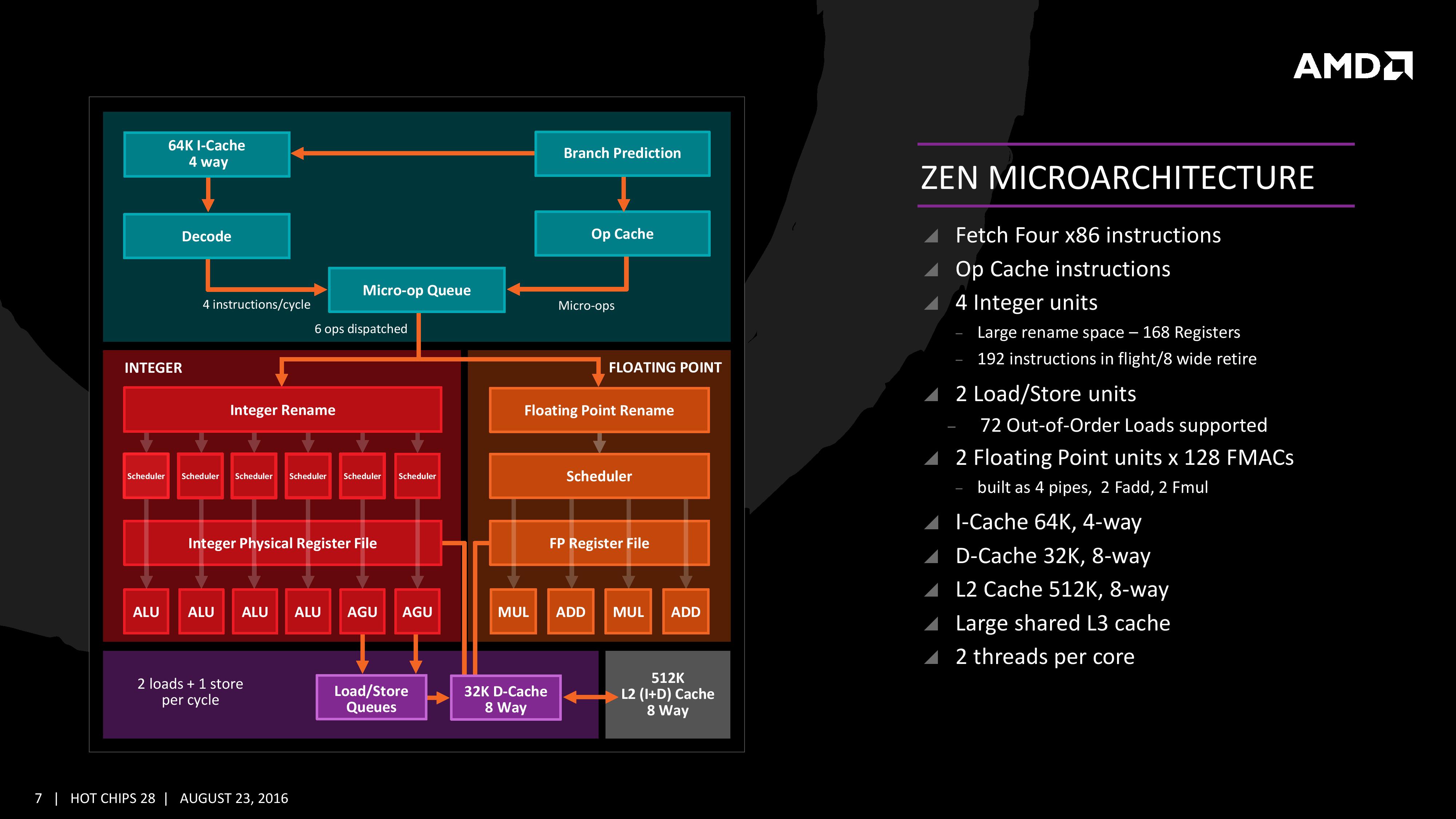
The improved branch predictor allows for 2 branches per Branch Target Buffer (BTB), but in the event of tagged instructions will filter through the micro-op cache. On the other side, the decoder can dispatch 4 instructions per cycle however some of those instructions can be fused into the micro-op queue. Fused instructions still come out of the queue as two micro-ops, but take up less buffer space as a result.
As mentioned earlier, the INT and FP pipes and schedulers are separated, but the INT rename space is 168 registers wide, which feeds into 6x14 scheduling queues. The FP employs as 160 entry register file, and both the FP and INT sections feed into a 192-entry retire queue. The retire queue can operate at 8 instructions per cycle, moving up from 4/cycle in previous AMD microarchitectures.
The load/store units are improved, supporting a 72 out-of-order loads, similar to Skylake. We’ll discuss this a bit later. On the FP side there are four pipes (compared to three in previous designs) which support combined 128-bit FMAC instructions. These cannot be combined for one 256-bit AVX2, but can be scheduled for AVX2 over two instructions.


106 Comments
View All Comments
extide - Monday, August 29, 2016 - link
No,k dude, it's not the same 4 ALU's, it's 4 ALU's per core. 2 threads a core, so 2 ALU's/thread, up to 16 threads, or 4 ALU's /thread up to 8 threads, but I would think it would be hard for a single thread to use 4 ALU's, so having 2 threads per 4 ALU seems fine, plus all the INT execution resources.Outlander_04 - Thursday, August 25, 2016 - link
40% improvement is not over Bulldozer but over Excavator which is already 20% or more ahead of Bulldozerlooncraz - Wednesday, August 24, 2016 - link
Highly scalar code or vector code will exceed 40% easily. The core execution resources relative to that execution is 75% to 100% greater. That will only translate to 50~60% performance improvement for said code, but a larger impact than the overall 40% improvement.The cache system, schedulers, issue width, AGUs, L/S, and other factors come more into play in the more common code paths, which reduces the maximum potential benefit derived from the additional execution resources.
However, multi-threaded performance should be HIGHER, not lower. Excavator had relatively poor MT scaling, Zen will be worlds better. Add SMT to the mix - and AMD's solution looks nearly exactly as I anticipated - and you have another 20% or so better SMT scaling.
It is easily conceivable, given what we now know, that AMD has met Haswell's average IPC outside of wider AVX workloads, and exceeded it in certain areas with heavy mixed compute (floating and integer concurrently). It is also now conceivable that AMD's first SMT implementation will be better than Intel's Sandy Bridge era Hyper-Threading. I didn't expect that at all, but the core flexibility is far ahead of Intel's flexibility - and that is largely what determines SMT performance in Zen's design.
Finally, <3Ghz @ 200W is way worse than the currently known figures for their 8C parts. They have 3.2Ghz boost clocks and just 95W TDP. It is expected that the clocks will increase, particularly for the quad core, 65W, parts.
You may not realize this, but these numbers put AMD slightly ahead of Intel in perf/W on 14nm.
niva - Wednesday, August 24, 2016 - link
So are you telling me my Phenom 2 black edition rig might be getting a worthy upgrade?I'm with you, but I don't trust these benchmarks, wait until the retail CPU samples are out then we can decide.
looncraz - Wednesday, August 24, 2016 - link
I'm saying you'll be able to match that level of performance with a Dual core Zen CPU w/ SMT... if AMD were actually to make one (doubtful).I do expect AMD to release triple core CPUs again, though, but possibly not right away.
Myrandex - Thursday, August 25, 2016 - link
Yay finally I've been holding onto my Phenom II as well and this might be it! :)Bulat Ziganshin - Thursday, August 25, 2016 - link
For vector code - they added 4'th ALU, it's almost nothing (Skylake added 4th scalar ALU and got laughable +3% IPC).For scalar code - they advertize +40% IPC. I'm pretty sure that they advertize the best part of perfromance, not the average one. It's ADVERTIZEMENT, after all.
Now, it's easy to analyze Zen as Carrizo+. M/t performance shouldn't change much since it's still 4-wide core (which was called module in Carrizo). S/t performance should improve much more since it changed from 2 alu to 4 alu. Overall, the core looks like Skylake, but it's not enough to put a lot of resources - they need to be carefully placed. Intel gone a long way optimizing their CPUs, and AMD have to repeat that. If you think that AMD can make Skylake-speed CPU in 2 years, then ask yourself - why Intel hasn't done the same in 2008 or so? Why IBM, having WIDER cpu, still slower than Intel in s/t tests?
All we know that AMD was able to SELECT single CPU that was able to run at 3 GHz using cooler looking like one they ship with 95W cpus. Just ask yourself - why they not tried to run their cpu at the same 3.2 GHz which is stock freq. for Intel CPU? And yes, it's way more effificent than Intel CPUs can, making me highly suspicious.
In one of pictures here AMD claims that Zen has the same power usage as Carrizo, that is 28nm CPU. AFAIR Carrizo with 2 modules at ~3GHz use 35-65 Wt. Multiple it by 4, please.
> It is also now conceivable that AMD's first SMT implementation will be better than Intel's Sandy Bridge era Hyper-Threading.
Why?? Intel's first SMT implementation in Pentium4 made a few percents improvement (over s/t), second one in Nehalem give me +20% on deflate, Sandy was +40%, and Haswell is +50%. Why you think that FIRST AMD attempt on SMT will be better than Pentium4?
Overall, i think that m/t perfromance of Zen is more predictable - it's Carrizo with some improvements, but still 4-wide, so i expect usual 10-20% generation-to-generation improvement.
For s/t, it less predictable, but i'm sure that it's impossible to beat Intel in single step, and AMD already advertized +40%, which i'm sure is about s/t perfromance.
looncraz - Thursday, August 25, 2016 - link
"For vector code - they added 4'th ALU, it's almost nothing (Skylake added 4th scalar ALU and got laughable +3% IPC)."Well, that was the average program performance increase, but the vector code itself sped up more than that.
Also, Zen's ability to leverage its resources should be better than Intel's, but its scheduler setup is really unique, so we need more details on how it will handle holes in a scheduler when its neighbor is full. Having six 14-deep schedulers is a significant part of the design that is almost completely overlooked, IMHO.
"Now, it's easy to analyze Zen as Carrizo+. M/t performance shouldn't change much since it's still 4-wide core"
Only if you are comparing a full module to a single Zen core... There were many bottlenecks in the modules that prevented full performance for multi-threading - Zen does not have that. On top, Zen has SMT, so it will have even better MT performance per core.
"Why IBM, having WIDER cpu, still slower than Intel in s/t tests?"
The width is, as you say, only a part of the equation. It's all about being able to exploit that extra width. Intel does so decently well, but has restrictions as a result of their unified scheduler. A heavy FPU load reduces integer performance, for example, due to shared ports of the scheduler. The impact of this is not easily quantifiable - it would require some very specialized testing. Zen will not have this issue thanks to dedicated schedulers.
Intel uses their unified scheduler to be able to provide results more quickly to dependent instructions. Zen, from appearances, allows each scheduler to make fetch and load requests directly, thereby nullifying what used to be an Intel advantage - and maybe even turning it into a hindrance.
"Just ask yourself - why they not tried to run their cpu at the same 3.2 GHz which is stock freq. for Intel CPU?"
Because you don't push engineering sample CPUs, and 3Ghz is the defacto industry standard speed for IPC comparison testing. Just look around, you'll find 3Ghz is the most commonly chosen frequency when doing IPC comparisons on modern CPUs. Pushing both to 3.2Ghz would not have changed anything, but a Zen engineering sample chip is worth thousands more than that Intel CPU at this time, and is not easily replaceable. If you have to run 500 more tests with it, and hand it over to other departments or teams, you probably aren't being allowed to overclock it any.
deltaFx2 - Friday, August 26, 2016 - link
The answer to the IBM question is easy. 1) IBM designed the Power8 with SMT-2 as the sweet spot. Like bulldozer, or Alpha EV6, they have execution clusters. In 2T, each cluster runs a thread, in 1T, the thread is split across these clusters, with a penalty for moving between them. Hence their 1T->2T uplift is a lot higher than intel's 1T->2T (worse baseline). (2) You're comparing different ISAs. x86 is a lot more CISC'y than POWER. x86 supports load+compute, compute+store, load+compute+store, and this is dispatched as a single uop. The same "work" in a more RISC'y machine needs 2 or 3 uops. For the same reason, an ARM core that hopes to achieve the same performance as x86 will need to dispatch more ops, or fuse more ops before dispatch.Spunjji - Saturday, August 27, 2016 - link
The CPU they tasted with is an early engineering sample. Simple answer. You write a lot to make yourself sound smart but you're exercising either clear bias or ignorance here.