AMD Zen Microarchiture Part 2: Extracting Instruction-Level Parallelism
by Ian Cutress on August 23, 2016 8:45 PM EST- Posted in
- CPUs
- AMD
- x86
- Zen
- Microarchitecture
The High-Level Zen Overview
AMD is keen to stress that the Zen project had three main goals: core, cache and power. The power aspect of the design is one that was very aggressive – not in the sense of aiming for a mobile-first design, but efficiency at the higher performance levels was key in order to be competitive again. It is worth noting that AMD did not mention ‘die size’ in any of the three main goals, which is usually a requirement as well. Arguably you can make a massive core design to run at high performance and low latency, but it comes at the expense of die size which makes the cost of such a design from a product standpoint less economical (if AMD had to rely on 500mm2 die designs in consumer at 14nm, they would be priced way too high). Nevertheless, power was the main concern rather than pure performance or function, which have been typical AMD targets in the past. The shifting of the goal posts was part of the process to creating Zen.
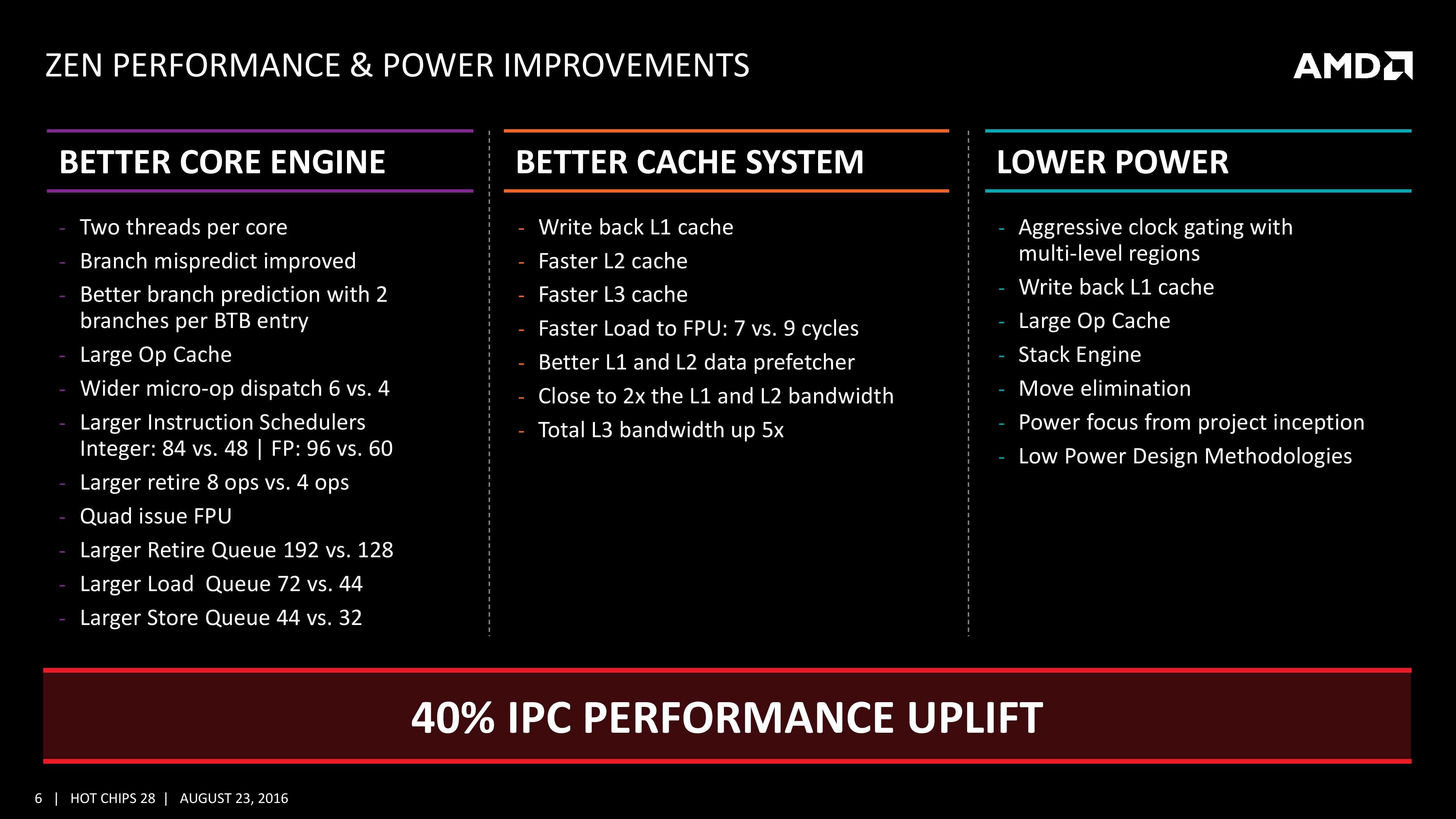
This slide contains a number of features we will hit on later in this piece but covers a number of main topics which come under those main three goals of core, cache and power.
For the core, having bigger and wider everything was to be expected, however maintaining a low latency can be difficult. Features such as the micro-op cache help most instruction streams improve in performance and bypass parts of potentially long-cycle repetitive operations, but also the larger dispatch, larger retire, larger schedulers and better branch prediction means that higher throughput can be maintained longer and in the fastest order possible. Add in dual threads and the applicability of keeping the functional units occupied with full queues also improves multi-threaded performance.
For the caches, having a faster prefetch and better algorithms ensures the data is ready when each of the caches when a thread needs it. Aiming for faster caches was AMD’s target, and while they are not disclosing latencies or bandwidth at this time, we are being told that L1/L2 bandwidth is doubled with L3 up to 5x.
For the power, AMD has taken what it learned with Carrizo and moved it forward. This involves more aggressive monitoring of critical paths around the core, and better control of the frequency and power in various regions of the silicon. Zen will have more clock regions (it seems various parts of the back-end and front-end can be gated as needed) with features that help improve power efficiency, such as the micro-op cache, the Stack Engine (dedicated low power address manipulation unit) and Move elimination (low-power method for register adjustment - pointers to registers are adjusted rather than going through the high-power scheduler).
The Big Core Diagram
We saw this diagram last week, but now we get updates on some of the bigger features AMD wants to promote:
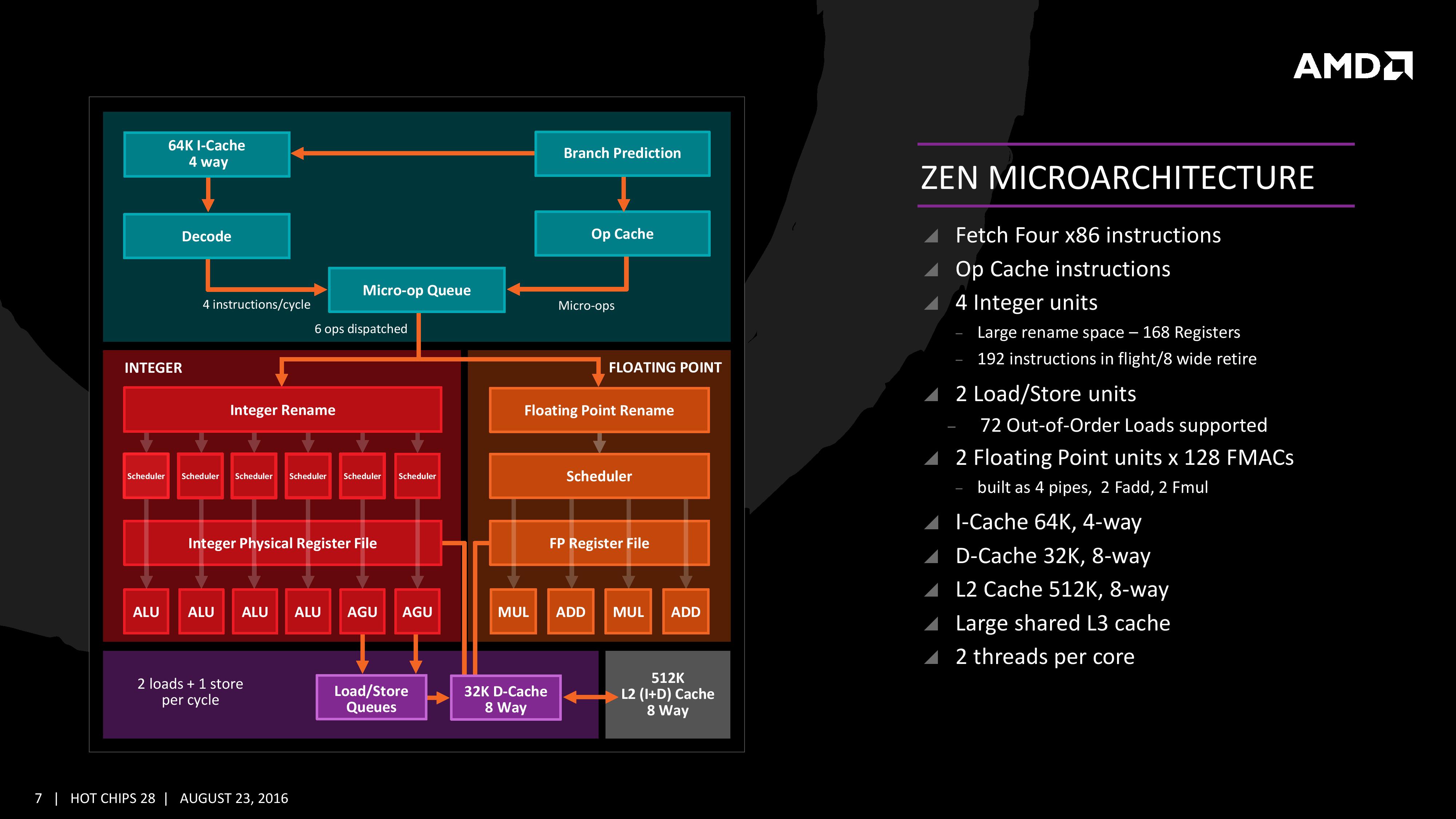
The improved branch predictor allows for 2 branches per Branch Target Buffer (BTB), but in the event of tagged instructions will filter through the micro-op cache. On the other side, the decoder can dispatch 4 instructions per cycle however some of those instructions can be fused into the micro-op queue. Fused instructions still come out of the queue as two micro-ops, but take up less buffer space as a result.
As mentioned earlier, the INT and FP pipes and schedulers are separated, but the INT rename space is 168 registers wide, which feeds into 6x14 scheduling queues. The FP employs as 160 entry register file, and both the FP and INT sections feed into a 192-entry retire queue. The retire queue can operate at 8 instructions per cycle, moving up from 4/cycle in previous AMD microarchitectures.
The load/store units are improved, supporting a 72 out-of-order loads, similar to Skylake. We’ll discuss this a bit later. On the FP side there are four pipes (compared to three in previous designs) which support combined 128-bit FMAC instructions. These cannot be combined for one 256-bit AVX2, but can be scheduled for AVX2 over two instructions.


106 Comments
View All Comments
Xajel - Wednesday, August 24, 2016 - link
I have a feeling that the Socket has more potential, there's a huge jump in pin counts that might hides something, I suspect AMD have specific HEDT version with higher TDP ( like 130-140 ) that might ship later in 2017 after the first wave. or maybe even triple channel that works only on higher-end HEDT motherboard while it will be still backward compatible with regular dual channels motherboards...none12345 - Wednesday, August 24, 2016 - link
Nice article, thanks, and timely too.Cant wait for real zen benchmarks.
I so badly want this to be another athlon64 x2 moment. But i dont think we will get that, and we don't need that. Consider the athlon 64 gave us multicore, and it stomped the pentium4 as well.
Ill be completey happy with a phenom II moment. Which was note quite as fast as intel, but gave you more almost as fast cores for your money. As well as unlocking cores at a much lower price point, which gave you superior overclocking for your money.
I will not at this point consider buying another quad core. Quad core is insufficient for my typical work load. I do not use 1 heavily multithreaded piece of software, i constantly use multiple pieces of moderately threaded software that currently mostly maxes out my processor.
In my opinion the industry should have stopped selling dual cores a year ago. It should be quad core at the low end and 6 or 8 core should be the mainstream. For desktop that is, i can still see some moble things being dual core.
Because i will NOT consider another quad core at this point. My only option today is the intel's enthusiast platform, which is far too expensive relative to the performance increase. So they are out.
And this is why im hoping that zen does not disappoint. If they can give me 6 or 8 cores that are within 10% per core, for similar costs to the i5 or i7 line, then im a definite buy. If they give me 6 or 8 cores that are priced like intel's enthusiast platform, well then i guess im not upgrading, untill someone can offer me more cores for a reasonable price.
If intel would offer more cores mainstream, then id absolutely consider a new chip from them. IE if i3 was 4 core, i5 was 6 core, and i7 was 8 core.
Vlad_Da_Great - Wednesday, August 24, 2016 - link
i7-4790K will wipe the floor with the ZEN mop. Roy Jones Jr(Intel) vs Montell Griffin(AMD) part II. https://www.youtube.com/watch?v=VZ_4FrhHHJE That is it! I cant believe AnandTech is biting on their marketing fluff.H2323 - Wednesday, August 24, 2016 - link
"Nevertheless, power was the main concern rather than pure performance or function, which have been typical AMD targets in the past."This is contradictory to what AMD has had to say. Power was not a greater focus than performance, just not true.
takeshi7 - Wednesday, August 24, 2016 - link
Wow, I haven't seen victim caches being used in a CPU since the old VIA C3. I hope the advantage of not having to duplicate data between the L2 and L3 caches pays off for AMD.H2323 - Wednesday, August 24, 2016 - link
and bulldozer in 2011Oxford Guy - Saturday, August 27, 2016 - link
The EDRAM L4 in Broadwell C is supposed to be a victim cache.intangir - Wednesday, August 24, 2016 - link
Great article. By the way, Ian, you're missing a syllable from "Microarchitecture" in the title.name99 - Wednesday, August 24, 2016 - link
"The first, CLZERO, is aimed to clear a cache line and is more aimed at the data center and HPC crowds"Not exactly. The point of an instruction like CLZERO is that the usual way cache lines are filled uses twice as much bandwidth as necessary.
When I write the first datum to a cacheline, the first thing that needs to be done is to load the cacheline and then overwrite the datum I wanted to write. This is obvious. BUT suppose I'm writing enough data that I write over the entire cache line? Then pulling it in was a waste of bandwidth.
THAT is the point of an instruction like CLZERO, to "ready the cache line for being overwritten" without wasting time loading it. Of course for many purposes filling with zeros is what one wants, but there are other times when one is simply engaged in bulk writing and it again makes sense.
PPC for example had a similar instruction, DCBZ, as does ARM, DC ZVA.
I'd expect this instruction to be used, at the absolute minimum, by the OS wherever it needs to zero and copy pages, by standard libraries data copy routines, and by the compiler whenever it writes "large" (ie cache line or larger) data structures.
"PTE (Page Table Entry) Coalescing is the ability to combine small 4K page tables into 32K page tables, and is a software transparent implementation. This is useful for reducing the number of entries in the TLBs and the queues, but requires certain criteria of the data to be used within the branch predictor to be met."
I think you are misunderstanding what this is about. My GUESS (only a guess) is that it refers to the following.
Academic work was done a few years ago that showed that the way Linux (and probably most other OSs) allocated and deallocated pages meant that, for the most part, contiguous virtual pages remain as contiguous physical pages over reasonably long stretches (say 8 to 16 pages). A consequence of this is that a TLB entry could contain not just the single physical address it refers to but also a length field or something equivalent, say that this TLB holds for this page and, say, the next 5 pages. This would work IF
- the pages all have the same settings and permissions (usually the case)
- the pages are contiguous in physical memory (as I said, usually the case)
The consequence of this is that for fairly minor modifications to the TLB, one manages to double or more the coverage of one's TLB, and that's certainly nothing to be sneered at.
It's possible that an OS that tries to maintain page contiguity could do even better --- the papers I read referred to unmodified Linux.
I've no idea what that branch predictor info refers to; but perhaps this is more of the usual x86 BS where you have to deal with some insane corner condition involving self-modifying code. The basic point, however, is obvious --- you get a nice increase in TLB coverage without having to change software, and without the pain of jumping to a larger page size.
I'm really glad to see AMD implement this because I thought it was a nice idea when I read it, and it's basically useful for everyone ---also IBM, also Intel, also ARM --- as long as the OS you're running is not insane. For someone like Apple, where they can fully control the OS, it's especially appealing. (And hell, for all we know they're actually first before AMD, they just never told anyone?)
name99 - Wednesday, August 24, 2016 - link
here we are, this is the paper I was referring to:http://www.cs.rutgers.edu/~abhib/binhpham-micro12....