AMD Zen Microarchiture Part 2: Extracting Instruction-Level Parallelism
by Ian Cutress on August 23, 2016 8:45 PM EST- Posted in
- CPUs
- AMD
- x86
- Zen
- Microarchitecture
Hot Chips is an annual conference that allows semiconductor companies to present their latest and greatest ideas or forthcoming products in an academic-style environment, and is predominantly aimed as the professional semiconductor engineer. This year has a number of talks about power management, upcoming IBM CPUs, upcoming Intel CPUs, upcoming NVIDIA SoCs and the final talk of the final day is from AMD, discussing Zen in even more depth than the previous week. While we were unable to attend the event in person, we managed to get some hands on time with information and put questions to Mike Clark, AMD Senior Fellow and design engineer.
What We Learned Last Week: L1/L2/L3 Caches and the Micro-Op Buffer
In AMD’s initial presentation for the general media, we were given a sense of the microarchitecture layout. We covered the material, but it contained a number of highlights.
AMD Zen Microarchitecture: Dual Schedulers, Micro-op Cache and Memory Hierarchy Revealed
AMD Server CPUs and Motherboard Analysis
Unpacking AMD's Zen Benchmark: Is Zen actually 2% Faster than Broadwell?
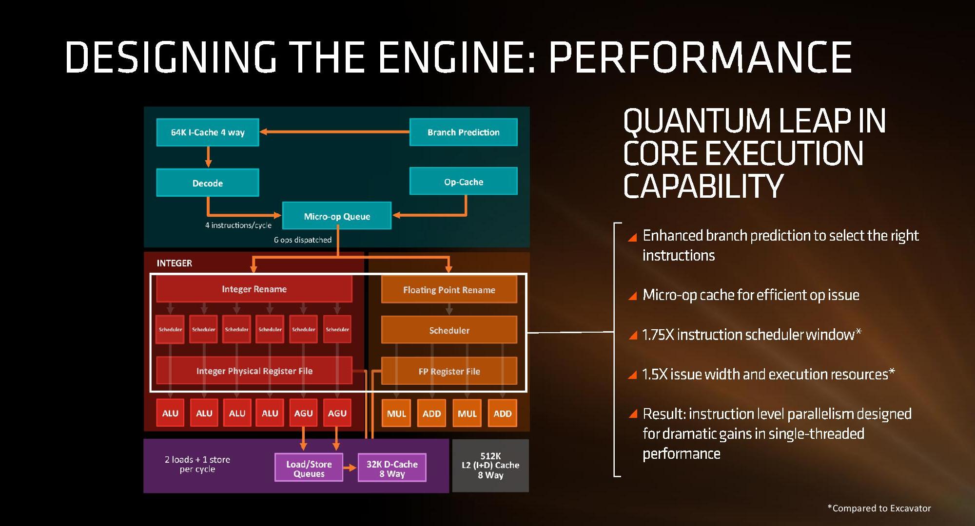
First up, and the most important, was the announcement of the inclusion of a micro-op cache. This allows for instructions that are frequently used to be closer to the micro-op queue and saves a trip through the core and caches to load the desired information. Typically micro-op caches are still relatively small, and while AMD isn’t giving any information for size and accessibility, we know that Intel’s version can support 1536 uOps with 8-way associativity; we expect AMD’s to be similar though there are many options in play.
Secondly is the cache structure. We were given details for the L1, L2 and L3 cache sizes, along with associativity, to compare it to former microarchitectures as well as Intel’s offering.
| CPU Cache Comparison | |||||
| Zen HEDT |
Bulldozer HEDT |
Excavator |
Skylake | Broadwell HEDT |
|
| L1-I | 64KB/core | 64KB/module | 96KB/module | 32KB/core | 32KB/core |
| 4-way | 2-way | 3-way | 8-way | 8-way | |
| L1-D | 32KB/core | 16KB/thread | 32KB/thread | 32KB/core | 32KB/core |
| 8-way | 4-way | 8-way | 8-way | 8-way | |
| L2 | 512KB/core | 1MB/thread | 512KB/thread | 256KB/core | 256KB/core |
| 8-way | 16-way | 16-way | 4-way | 8-way | |
| L3 | 2MB/core | 1MB/thread | - | >2MB/core | 1.5-3MB/core |
| 16-way | 64-way | - | 16-way | 16/20-way | |
| L3 Type | Victim | Victim | - | Write-back | Write-back |
In this case, AMD has given Zen a 64KB L1 Instruction cache per core with 4-way associativity, with a lop-sided 32KB L1 Data cache per core with 8-way associativity. The size and accessibility determines how frequently a cache line is missed, and it is typically a trade-off for die area and power (larger caches require more die area, more associativity usually costs power). The instruction cache, per cycle, can afford a 32byte fetch while the data cache allows for 2x 16-byte loads and one 16-byte store per cycle. AMD stated that allowing two D-cache loads per cycle is more representative of the most workloads that end up with more loads than stores.
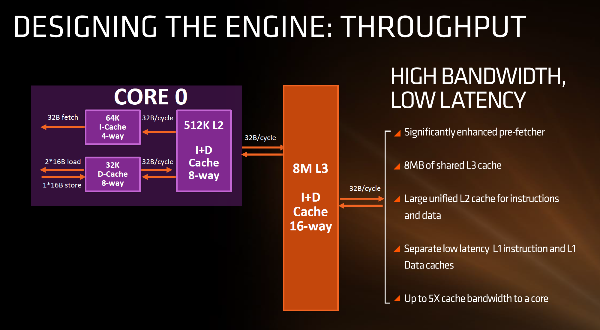
The L2 is a large 512 KB, 8-way cache per core. This is double the size of Intel’s 256 KB 4-way cache in Skylake or 256 KB 8-way cache in Broadwell. Typically doubling the cache size affords a 1.414 (square root of 2) better chance of a cache hit, reducing the need to go further out to find data, but comes at the expense of die area. This will have a big impact on a lot of performance metrics, and AMD is promoting faster cache-to-cache transfers than previous generations. Both the L1 and L2 caches are write-back caches, improving over the L1 write-through cache in Bulldozer.
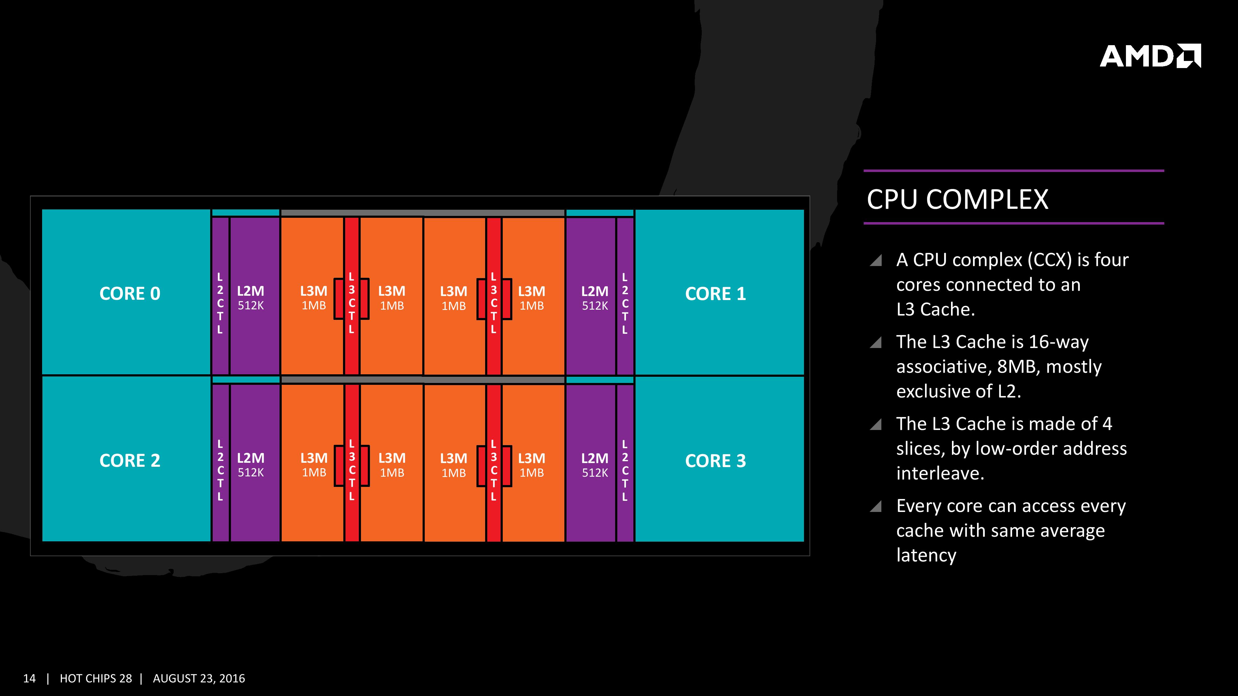
The L3 cache is an 8MB 16-way cache, although at the time last week it was not specified over how many cores this was. From the data release today, we can confirm rumors that this 8 MB cache is split over a four-core module, affording 2 MB of L3 cache per core or 16 MB of L3 cache for the whole 8-core Zen CPU. These two 8 MB caches are separate, so act as a last-level cache per 4-core module with the appropriate hooks into the other L3 to determine if data is needed. As part of the talk today we also learned that the L3 is a pure victim cache for L1/L2 victims, rather than a cache for prefetch/demand data, which tempers the expectations a little but the large L2 will make up for this. We’ll discuss it as part of today’s announcement.
The mid-week release also gave insight into the dual schedulers, one for INT and another for FP, which is different to Intel’s joint scheduler/buffer implementation. The talk at Hot Chips goes into detail about how the dispatch and schedulers operate
The New Information
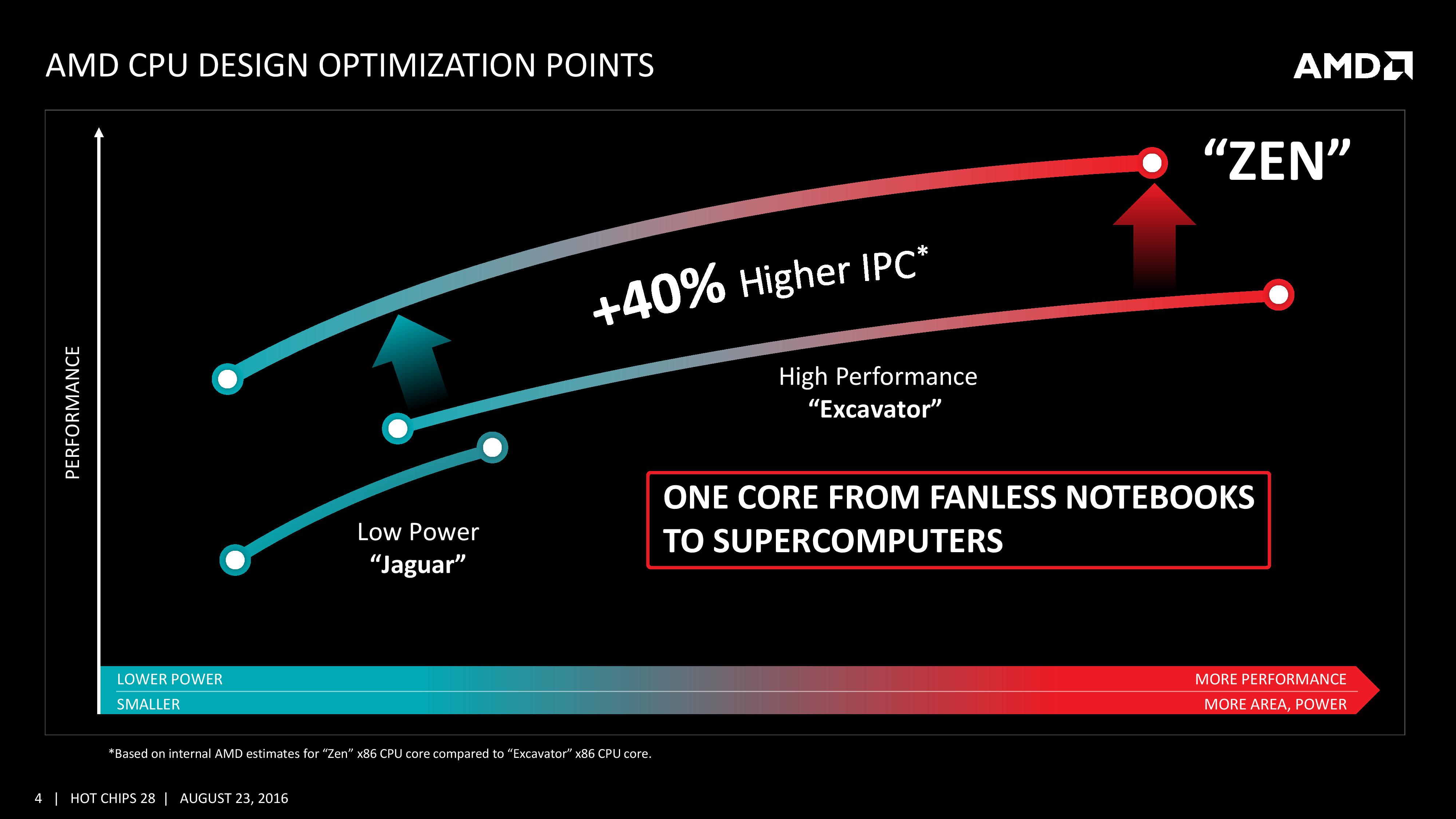
As part of the Hot Chips presentation, AMD is reaffirming its commitment to at least +40% IPC improvement over Excavator. This has specifically been listed as a throughput goal at an equivalent energy per cycle, resulting in an increase in efficiency. Obviously a number of benefits come from moving the 28nm TSMC process to GloFo’s 14nm FinFET process which is used via a Samsung licence. Both the smaller node and FinFET improvements have been well documented so we won’t go over them here, but AMD is stating that Zen is much more than this as a direct improvement to immediate performance, not just efficiency. While Zen is initially a high-performance x86 core at heart, it is designed to scale all the way from notebooks to supercomputers, or from where the Cat cores (such as Jaguar and Puma) were all the way up to the old Opterons and beyond, all with at least +40% IPC.
The first immediate image out of the presentation is the CPU Complex (a CCX), which shows the Zen core design as a four-CPU cluster with caches. This shows the L2/L3 cache breakdown, and also confirms 2MB of L3 per core with 8 MB of L3 per CCX. It also states that the L3 is mostly exclusive of the L2 cache, which stems from the L3 cache as a victim cache for L2 data. AMD is stating that the protocols involved in the L3 cache design allow each core to access the L3 of each other core with an average (but a range) of latencies.
Over the next few pages, we’ll go through the slides. They detail more information about the application of Simultaneous Multithreading (SMT), New Instructions, the size of various queues and buffers, the back-end of the design, the front-end of the design, fetch, decode, execute, load/store and retire segments.


106 Comments
View All Comments
Xajel - Wednesday, August 24, 2016 - link
I have a feeling that the Socket has more potential, there's a huge jump in pin counts that might hides something, I suspect AMD have specific HEDT version with higher TDP ( like 130-140 ) that might ship later in 2017 after the first wave. or maybe even triple channel that works only on higher-end HEDT motherboard while it will be still backward compatible with regular dual channels motherboards...none12345 - Wednesday, August 24, 2016 - link
Nice article, thanks, and timely too.Cant wait for real zen benchmarks.
I so badly want this to be another athlon64 x2 moment. But i dont think we will get that, and we don't need that. Consider the athlon 64 gave us multicore, and it stomped the pentium4 as well.
Ill be completey happy with a phenom II moment. Which was note quite as fast as intel, but gave you more almost as fast cores for your money. As well as unlocking cores at a much lower price point, which gave you superior overclocking for your money.
I will not at this point consider buying another quad core. Quad core is insufficient for my typical work load. I do not use 1 heavily multithreaded piece of software, i constantly use multiple pieces of moderately threaded software that currently mostly maxes out my processor.
In my opinion the industry should have stopped selling dual cores a year ago. It should be quad core at the low end and 6 or 8 core should be the mainstream. For desktop that is, i can still see some moble things being dual core.
Because i will NOT consider another quad core at this point. My only option today is the intel's enthusiast platform, which is far too expensive relative to the performance increase. So they are out.
And this is why im hoping that zen does not disappoint. If they can give me 6 or 8 cores that are within 10% per core, for similar costs to the i5 or i7 line, then im a definite buy. If they give me 6 or 8 cores that are priced like intel's enthusiast platform, well then i guess im not upgrading, untill someone can offer me more cores for a reasonable price.
If intel would offer more cores mainstream, then id absolutely consider a new chip from them. IE if i3 was 4 core, i5 was 6 core, and i7 was 8 core.
Vlad_Da_Great - Wednesday, August 24, 2016 - link
i7-4790K will wipe the floor with the ZEN mop. Roy Jones Jr(Intel) vs Montell Griffin(AMD) part II. https://www.youtube.com/watch?v=VZ_4FrhHHJE That is it! I cant believe AnandTech is biting on their marketing fluff.H2323 - Wednesday, August 24, 2016 - link
"Nevertheless, power was the main concern rather than pure performance or function, which have been typical AMD targets in the past."This is contradictory to what AMD has had to say. Power was not a greater focus than performance, just not true.
takeshi7 - Wednesday, August 24, 2016 - link
Wow, I haven't seen victim caches being used in a CPU since the old VIA C3. I hope the advantage of not having to duplicate data between the L2 and L3 caches pays off for AMD.H2323 - Wednesday, August 24, 2016 - link
and bulldozer in 2011Oxford Guy - Saturday, August 27, 2016 - link
The EDRAM L4 in Broadwell C is supposed to be a victim cache.intangir - Wednesday, August 24, 2016 - link
Great article. By the way, Ian, you're missing a syllable from "Microarchitecture" in the title.name99 - Wednesday, August 24, 2016 - link
"The first, CLZERO, is aimed to clear a cache line and is more aimed at the data center and HPC crowds"Not exactly. The point of an instruction like CLZERO is that the usual way cache lines are filled uses twice as much bandwidth as necessary.
When I write the first datum to a cacheline, the first thing that needs to be done is to load the cacheline and then overwrite the datum I wanted to write. This is obvious. BUT suppose I'm writing enough data that I write over the entire cache line? Then pulling it in was a waste of bandwidth.
THAT is the point of an instruction like CLZERO, to "ready the cache line for being overwritten" without wasting time loading it. Of course for many purposes filling with zeros is what one wants, but there are other times when one is simply engaged in bulk writing and it again makes sense.
PPC for example had a similar instruction, DCBZ, as does ARM, DC ZVA.
I'd expect this instruction to be used, at the absolute minimum, by the OS wherever it needs to zero and copy pages, by standard libraries data copy routines, and by the compiler whenever it writes "large" (ie cache line or larger) data structures.
"PTE (Page Table Entry) Coalescing is the ability to combine small 4K page tables into 32K page tables, and is a software transparent implementation. This is useful for reducing the number of entries in the TLBs and the queues, but requires certain criteria of the data to be used within the branch predictor to be met."
I think you are misunderstanding what this is about. My GUESS (only a guess) is that it refers to the following.
Academic work was done a few years ago that showed that the way Linux (and probably most other OSs) allocated and deallocated pages meant that, for the most part, contiguous virtual pages remain as contiguous physical pages over reasonably long stretches (say 8 to 16 pages). A consequence of this is that a TLB entry could contain not just the single physical address it refers to but also a length field or something equivalent, say that this TLB holds for this page and, say, the next 5 pages. This would work IF
- the pages all have the same settings and permissions (usually the case)
- the pages are contiguous in physical memory (as I said, usually the case)
The consequence of this is that for fairly minor modifications to the TLB, one manages to double or more the coverage of one's TLB, and that's certainly nothing to be sneered at.
It's possible that an OS that tries to maintain page contiguity could do even better --- the papers I read referred to unmodified Linux.
I've no idea what that branch predictor info refers to; but perhaps this is more of the usual x86 BS where you have to deal with some insane corner condition involving self-modifying code. The basic point, however, is obvious --- you get a nice increase in TLB coverage without having to change software, and without the pain of jumping to a larger page size.
I'm really glad to see AMD implement this because I thought it was a nice idea when I read it, and it's basically useful for everyone ---also IBM, also Intel, also ARM --- as long as the OS you're running is not insane. For someone like Apple, where they can fully control the OS, it's especially appealing. (And hell, for all we know they're actually first before AMD, they just never told anyone?)
name99 - Wednesday, August 24, 2016 - link
here we are, this is the paper I was referring to:http://www.cs.rutgers.edu/~abhib/binhpham-micro12....