Ten Year Anniversary of Core 2 Duo and Conroe: Moore’s Law is Dead, Long Live Moore’s Law
by Ian Cutress on July 27, 2016 10:30 AM EST- Posted in
- CPUs
- Intel
- Core 2 Duo
- Conroe
- ITRS
- Nostalgia
- Time To Upgrade
Today marks a full 10 years since the first Core 2 Duo processors, and hence Intel’s 64-bit Core microarchitecture, were made officially available at retail. These included a number of popular dual-core processor parts, including the seemingly ubiquitous E6400 and the Core 2 Extreme X6800. These were built on Intel’s 65nm process, and marked a turning point in the desktop processor ecosystem. To quote Anand in our launch review: ‘you’re looking at the most impressive piece of silicon the world has ever seen’.
Ten Year Anniversary of Core 2 Duo and Conroe
As part of this piece we will also look at some of the predictions for the future, from the latest (and possibly last) International Technology Roadmap for Semiconductors report, which predicts the stalling of smaller silicon manufacturing nodes over the next 10-15 years.
The first part of this article borrows heavily from Johan’s original look into the Intel Core microarchitecture back in 2006. It’s an awesome read.
Back When I Were A Lad
For a number of our readers, the launch of Conroe was a vast change in the processing landscape. The family of Netburst, Northwood and Prescott processors, in the form of Pentium D and Pentium 4, showed that pursuing the frequency race pushed the silicon far outside its efficiency zone and left a hot, power hungry mess in its wake. It didn’t even come with a muscular V8 sound, and AMD’s Athlon 64 X2 line had taken both the performance and efficiency crown.
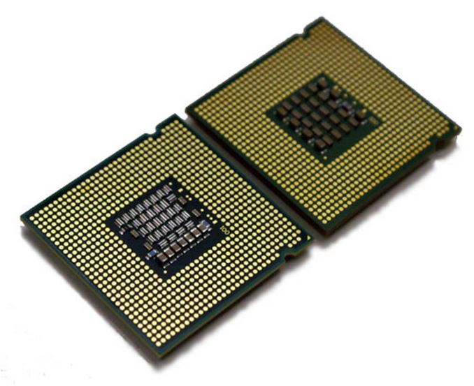
Core 2 Duo (left) vs Pentium D (right)
From the perspective of Intel, it had to incorporate a significant paradigm shift in the way it approached the core microarchitecture – no more long pipelines to bump up clock rates to start. The Core microarchitecture design was marketed as a blend of Pentium Pro and Pentium M techniques, as well as the Netburst architecture, however as Johan pointed out at the time, it is significantly Pentium M and it is very hard to find anything Netburst in there. It wasn’t as simple as ‘adding a few functional units or decoders on Yonah and calling it a day’, almost 80% of the architecture and circuit design had to be redone.
As part of this piece, we’re going to take another look at the original architecture improvements of the Core microarchitecture design and some of our old performance metrics from a decade ago.
27th July 2006: Core 2 Launch Day
Ten years ago, Intel launched the following five processors:
| CPU | Clock Speed | L2 Cache |
| Intel Core 2 Extreme X6800 | 2.93GHz | 4MB |
| Intel Core 2 Duo E6700 | 2.66GHz | 4MB |
| Intel Core 2 Duo E6600 | 2.40GHz | 4MB |
| Intel Core 2 Duo E6400 | 2.13GHz | 2MB |
| Intel Core 2 Duo E6300 | 1.86GHz | 2MB |
The X6800 sits at the top with a higher clock speed with a higher supported FSB-to-core ration than previous Intel processors. The Core 2 processors all came from a 143mm2 die, compared the 162mm2 of Pentium D, and they both seem tiny by comparison to the large die sizes we see 2016 for things like the P100. These were chips without integrated graphics either. The introduction of Core 2 pushed the prices of the Pentium D processors down, to give this interesting table:
| CPU | Clock Speed | L2 Cache | Price |
| Intel Core 2 Extreme X6800 | 2.93GHz | 4MB | $999 |
| Intel Core 2 Duo E6700 | 2.66GHz | 4MB | $530 |
| Intel Core 2 Duo E6600 | 2.40GHz | 4MB | $316 |
| Intel Core 2 Duo E6400 | 2.13GHz | 2MB | $224 |
| Intel Core 2 Duo E6300 | 1.86GHz | 2MB | $183 |
| Intel Pentium D 945 | 3.40GHz | 2MBx2 | $163 |
| Intel Pentium D 915 | 2.80GHz | 2MBx2 | $133 |
| Intel Pentium D 820 | 2.80GHz | 1MBx2 | $113 |
| Intel Pentium D 805 | 2.66GHz | 1MBx2 | $93 |
Comparing this to recent Intel processors, and the X8600 matches the list price of the Core i7-5960X (an 8-core part), whereas the popular Core 2 Duo E6400 at $224 at the same price as the Core i5-6600.
A few years ago, I salvaged a super old computer of mine with an E6400 and took it for a spin for a pipeline piece entitled ‘Dragging Core 2 Duo into 2013’. We know that a number of users today are still using the old platform as their day to day machine, and given that it is now celebrating its 10th birthday, it is interesting that anyone wanting to play around with the old hardware can get a motherboard, memory and CPU from eBay for $50-70.
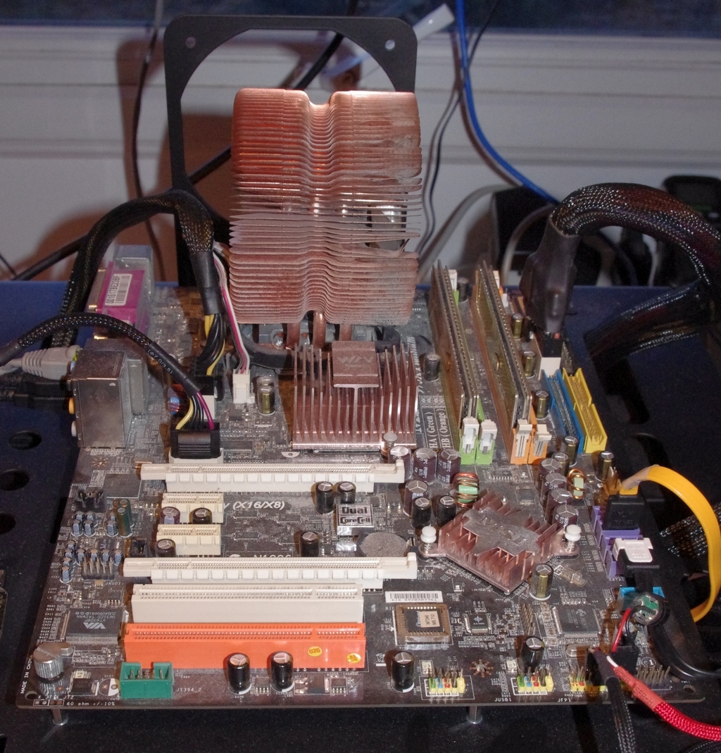
My crusty C2D Setup from 2013


158 Comments
View All Comments
Akrovah - Wednesday, July 27, 2016 - link
My old E6700 is still alive and kicking. I only just replaced it as my primary system when Devil's Canyon came along. Still use it for my four year old's "first computer."djayjp - Wednesday, July 27, 2016 - link
Not a particle physicist, nor electrical engineer, so just some pie in the sky wondering here, but wouldn't it be possible to build transistors using carbon nanotubes, or light itself (using nano sized mirrors/interferometers, like DLP) or even basing the transistor gates off of protons/sub atomic particles?michael2k - Wednesday, July 27, 2016 - link
I think a more interesting question is using glass as a substrate. Imagine printing nand, CPU, GPU, ram, and along the bezels of a smartphone.That reduces a phone to six components: a display, a transducer for sound, a mic, a battery, a radio, and a chassis, which would have all the antennas.
joex4444 - Wednesday, July 27, 2016 - link
Particle physicist here. Light has the tricky property that it travels at the speed of light so I can't imagine it working but perhaps I'm envisioning your concept differently than you are. For carbon nanotubes, you'll need a materials engineer or a condensed matter physicist.3DoubleD - Wednesday, July 27, 2016 - link
Materials/Semiconductor Physics Engineer here. The problem is not what we CAN do, the problem is what is economically possible at scale. For example, FinFETs were demonstrated at the turn of the century, but took all of those years to become (1) necessary - planar transistor were getting too leaky, and (2) possible to fabricate economically in large scales.Researchers have created smaller, faster transistors years ago, but it takes a lot of time and effort to develop the EUV or quadruple patterning technologies that enable these devices to be reliably and affordably manufactured.
So I think the problem in moving "beyond silicon" is not that we don't have alternatives, it is that we have many alternatives, we just don't know which will scale. It becomes less of a purely engineering problem and manufacturing business problem. When new technologies relied purely on the established silicon industry alone, you could reasonably extrapolate how much each new technology would cost as the nodes were scaled down. When we talk about using III-V FinFETs/ All Around Gates or graphene and carbon nanotubes, we don't really know how those things will scale with the existing processes as we move them from the laboratory to the manufacturing line.
I've been looking forward to this transition for years. People moan that it is the end of Moores Law, but that could be a good thing. Silicon is a great material for forming logic circuits for many reasons, but it also has many downsides. While silicon never reached 10 GHz (as Intel once predicted), other materials easily blow past 100 GHz transistor switching speeds. When the massive engines that work tirelessly to reduce our lithography nodes nm by nm are aimed at "the next big thing", we might be pleasantly surprised by a whole new paradigm of performance.
So what competes with modern day Si CMOS on speed, power usage, and cost? Nothing... yet!
djayjp - Thursday, July 28, 2016 - link
Yes, it's fascinating stuff. Thanks for reminding me about that. I recall now that I think it was graphene that enabled those insanely high switching speeds, due to its incredible conductivity/efficiency. Hopefully it can now be made economically feasible at some point! Imagine a the next GPU that is 10x smaller and operates at 100x the clock speed. A GTX 1080Ti x 1000! Finally we can do real time true global illumination ha....jeffry - Monday, August 1, 2016 - link
Thats a good point. Like, answering a question "are you willing to pay $800 for a new CPU to double the computers speed?" Most consumers say no. It all comes down to the mass market price.wumpus - Thursday, August 4, 2016 - link
From the birth of the Univac until 10 years ago, consumers consistently said YES! and plunked down their money. Doubling the (per thread) speed of a core2duo is going to cost more than $800. Also the cost of the RAM on servers is *WAY* more than $800, so you can expect if Intel could double the power of each core, they could crank prices up by at least $800 per core on Xeons. They can't, and neither can IBM or AMD.Jaybus - Thursday, July 28, 2016 - link
Sure, but that speed is dependent on the medium. There are some proposed optical transistors using electromagnetically induced transparency. Long way off. However, silicon photonics could change some things. Capacitance is the killer for electronic interconnects, whether chip-to-chip or on-chip bus. An optical interconnect could greatly increase bandwidth without increasing the chip's power dissipation. I think an electronic-photonic hybrid is more likely, since silicon photonics components can be made on a CMOS process. We are already beginning to see optical PCI Express being deployed. I could definitely see a 3D approach where 2D electronic layers are connected through an optical rather than electronic bus.djayjp - Thursday, July 28, 2016 - link
Yes, transparency, like polarized windows that either become transparent or opaque when a current is applied (to the liquid crystals?). I wonder how small they could be made. It would be incredibly power efficient I would think.