Ten Year Anniversary of Core 2 Duo and Conroe: Moore’s Law is Dead, Long Live Moore’s Law
by Ian Cutress on July 27, 2016 10:30 AM EST- Posted in
- CPUs
- Intel
- Core 2 Duo
- Conroe
- ITRS
- Nostalgia
- Time To Upgrade
Today marks a full 10 years since the first Core 2 Duo processors, and hence Intel’s 64-bit Core microarchitecture, were made officially available at retail. These included a number of popular dual-core processor parts, including the seemingly ubiquitous E6400 and the Core 2 Extreme X6800. These were built on Intel’s 65nm process, and marked a turning point in the desktop processor ecosystem. To quote Anand in our launch review: ‘you’re looking at the most impressive piece of silicon the world has ever seen’.
Ten Year Anniversary of Core 2 Duo and Conroe
As part of this piece we will also look at some of the predictions for the future, from the latest (and possibly last) International Technology Roadmap for Semiconductors report, which predicts the stalling of smaller silicon manufacturing nodes over the next 10-15 years.
The first part of this article borrows heavily from Johan’s original look into the Intel Core microarchitecture back in 2006. It’s an awesome read.
Back When I Were A Lad
For a number of our readers, the launch of Conroe was a vast change in the processing landscape. The family of Netburst, Northwood and Prescott processors, in the form of Pentium D and Pentium 4, showed that pursuing the frequency race pushed the silicon far outside its efficiency zone and left a hot, power hungry mess in its wake. It didn’t even come with a muscular V8 sound, and AMD’s Athlon 64 X2 line had taken both the performance and efficiency crown.
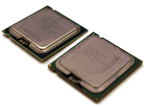
Core 2 Duo (left) vs Pentium D (right)
From the perspective of Intel, it had to incorporate a significant paradigm shift in the way it approached the core microarchitecture – no more long pipelines to bump up clock rates to start. The Core microarchitecture design was marketed as a blend of Pentium Pro and Pentium M techniques, as well as the Netburst architecture, however as Johan pointed out at the time, it is significantly Pentium M and it is very hard to find anything Netburst in there. It wasn’t as simple as ‘adding a few functional units or decoders on Yonah and calling it a day’, almost 80% of the architecture and circuit design had to be redone.
As part of this piece, we’re going to take another look at the original architecture improvements of the Core microarchitecture design and some of our old performance metrics from a decade ago.
27th July 2006: Core 2 Launch Day
Ten years ago, Intel launched the following five processors:
| CPU | Clock Speed | L2 Cache |
| Intel Core 2 Extreme X6800 | 2.93GHz | 4MB |
| Intel Core 2 Duo E6700 | 2.66GHz | 4MB |
| Intel Core 2 Duo E6600 | 2.40GHz | 4MB |
| Intel Core 2 Duo E6400 | 2.13GHz | 2MB |
| Intel Core 2 Duo E6300 | 1.86GHz | 2MB |
The X6800 sits at the top with a higher clock speed with a higher supported FSB-to-core ration than previous Intel processors. The Core 2 processors all came from a 143mm2 die, compared the 162mm2 of Pentium D, and they both seem tiny by comparison to the large die sizes we see 2016 for things like the P100. These were chips without integrated graphics either. The introduction of Core 2 pushed the prices of the Pentium D processors down, to give this interesting table:
| CPU | Clock Speed | L2 Cache | Price |
| Intel Core 2 Extreme X6800 | 2.93GHz | 4MB | $999 |
| Intel Core 2 Duo E6700 | 2.66GHz | 4MB | $530 |
| Intel Core 2 Duo E6600 | 2.40GHz | 4MB | $316 |
| Intel Core 2 Duo E6400 | 2.13GHz | 2MB | $224 |
| Intel Core 2 Duo E6300 | 1.86GHz | 2MB | $183 |
| Intel Pentium D 945 | 3.40GHz | 2MBx2 | $163 |
| Intel Pentium D 915 | 2.80GHz | 2MBx2 | $133 |
| Intel Pentium D 820 | 2.80GHz | 1MBx2 | $113 |
| Intel Pentium D 805 | 2.66GHz | 1MBx2 | $93 |
Comparing this to recent Intel processors, and the X8600 matches the list price of the Core i7-5960X (an 8-core part), whereas the popular Core 2 Duo E6400 at $224 at the same price as the Core i5-6600.
A few years ago, I salvaged a super old computer of mine with an E6400 and took it for a spin for a pipeline piece entitled ‘Dragging Core 2 Duo into 2013’. We know that a number of users today are still using the old platform as their day to day machine, and given that it is now celebrating its 10th birthday, it is interesting that anyone wanting to play around with the old hardware can get a motherboard, memory and CPU from eBay for $50-70.
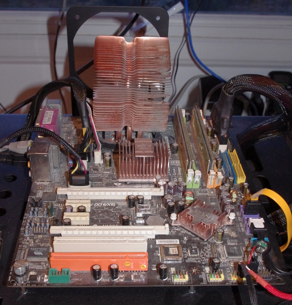
My crusty C2D Setup from 2013


158 Comments
View All Comments
Ian Cutress - Tuesday, August 2, 2016 - link
To clarify, there was a typo in Johan's original review of the microarchitecture, specifically stating:'However, Core is clearly a descendant of the Pentium Pro,'
I've updated the article to reflect this, and was under the assumption that my source was correct at the point of doing my research.
wumpus - Tuesday, August 2, 2016 - link
Except that the Pentium Pro was the first chip with the P6 architecture. Pentium 2 was pretty much pentium pro with MMX, a higher clock rate, and slower [off chip but on slot] L2 cache. Pentium 3 was the same with more clock, more MMX (possibly SSE), and on chip (full speed) L2 cache.While I'd have to assume they would pull all the files from the Pentium 3 plans, I'd still call it "pentinium pro based" because that was where nearly all the architecture came from (with minor upgrades and bug fixes to the core in 2 and 3).
I'm still curious as to exactly how they pulled it off. My main theory is that they duplicated the block diagram of the P6, and then verified each block was correct (and exactly duplicated the P6 at a higher speed), then used the P6 verification to prove that if the blocks were all correct, they had a correct chip.
zodiacfml - Thursday, July 28, 2016 - link
Same here. I thought it was the design of the Pentium M (from Israel team) they got the Core from. It was that time that AMD is beating Intel's P4's in performance, efficiency, and price. After a few months, articles were posted with people able to overclock a Pentium M with the characteristics of the AMD CPU and, of course, beating Pentium 4's at much lower clock speeds. From there, the Intel Core was born out of the Pentium M's which is essentially the same only with higher TDP and clock speeds. Then came, the Core Duo, then the Core 2 Duo.I just can't remember where I read it though.
marty1980 - Wednesday, July 27, 2016 - link
I started college in electrical engineering; moved to software after an ee class using c++. I was very excited and confident in a DIY PC. I knew the Core 2 was on its way. I gathered parts from whatever computers I could scratch together; power supply, case, DVD drive, network card(s), HDDs ... Everything but Mobo, CPU, GPU and RAM - the brains.I bought an E6400 2.13GHz with a gigabyte mobo, 4GB 800MHz DDR2 and a Radeon x1650 Pro.
I just retired the CPU and Mobo in 2012/13 when I experimented with my current PC; an AMD APU + Ded GPU (dual graphics).
I'm excited to be looking at a future replacement for my PC. We're on the horizon of some interesting changes that I don't even understand (what was his article about? Lol).
just4U - Thursday, July 28, 2016 - link
I seem to recall from a casual glance at an article (on this site) back some 9 years ago.. That intel basically got lucky, or fluked as it were.. Something to do with what they were doing with the PentiumM which caused them to move away from the P3-4 stuff.. hum.. damned if I can remember though what it was about.FourEyedGeek - Tuesday, August 9, 2016 - link
Pentium 3 architecture was having difficulties increasing performance so they replaced it with Pentium 4s Netburst. They had their Israel department continue work on Pentium 3 that turned into the Pentium M.Hazly79 - Thursday, July 28, 2016 - link
surprised that my 2005-Pentium D 3ghz still can run Diablo 3 (2012) at minimum setting pair with Nvidia GT 710 ($35 card )Really great optimization from Blizzard ent. team...
AnnonymousCoward - Thursday, July 28, 2016 - link
Yeah, but too bad the game sucks. Jay doubled it.name99 - Thursday, July 28, 2016 - link
Two points:Firstly macro-op fusion is hardly an x86 exclusive these days. Many (all?) ARMv8 CPUs use it, as do the most recent POWER CPUs. Like the x86 case, it's used to fuse together pairs of instructions that commonly co-occur. Compare and branch is a common example, but other common examples in RISC are instruction pairs that are used to create large constants in a register, or to generate large constant offsets for loads/stores.
Secondly you suggest that the ROB is an expensive data structure. This is misleading. The ROB itself is primarily a FIFO and can easily be grown. The problem is that storing more items in the ROB requires more physical registers and more load/store queue entries, and it is THESE structures that are difficult and expensive to grow. This suggests that using alternative structures for the load/store queues, and alternative mechanisms for scavenging physical registers could allow for much larger ROBs, and in fact Intel has published a lot of work on this (but has so far done apparently nothing with this research, even though the first such publications were late 90s --- I would not be surprised if Apple provides us with a CPU implementing these ideas before Intel does).
Ian Cutress - Tuesday, August 2, 2016 - link
It wasn't written about to the exclusion of all other microarchitectures, it was written about focusing on x86 back in 2006. At the time, the ROB was described as expensive by Intel, through I appreciate that might have changed.