Ten Year Anniversary of Core 2 Duo and Conroe: Moore’s Law is Dead, Long Live Moore’s Law
by Ian Cutress on July 27, 2016 10:30 AM EST- Posted in
- CPUs
- Intel
- Core 2 Duo
- Conroe
- ITRS
- Nostalgia
- Time To Upgrade
Core: It’s all in the Prefetch
In a simple CPU design, instructions are decoded in the core and data is fetched from the caches. In a perfect world, such as the Mill architecture, the data and instructions are ready to go in the lowest level cache at all times. This allows for the lowest latency and removes a potential bottleneck. Real life is not that rosy, and it all comes down to how the core can predict what data it needs and has enough time to drag it down to the lowest level of cache it can before it is needed. Ideally it needs to predict the correct data, and not interfere with memory sensitive programs. This is Prefetch.
The Core microarchitecture added multiple prefetchers in the design, as well as improving the prefetch algorithms, to something not seen before on a consumer core. For each core there are two data and one instruction prefetchers, plus another couple for the L2 cache. That’s a total of eight for a dual core CPU, with instructions not to interfere with ‘on-demand’ bandwidth from running software.
One other element to the prefetch is tag lookup for cache indexing. Data prefetchers do this, as well as running software, so in order to avoid a higher latency for the running program, the data prefetch uses the store port to do this. As a general rule (at least at the time), loads happen twice as often as stores, meaning that the store port is generally more ‘free’ to be used for tag lookup by the prefetchers. Stores aren’t critical for most performance metrics, unless the system can’t process stores quickly enough that it backs up the pipeline, but in most cases the rest of the core will be doing things regardless. The cache/memory sub-system is in control for committing the store through the caches, so as long as this happens eventually the process works out.
Core: More Cache Please
Without having access to a low latency data and instruction store, having a fast core is almost worthless. The most expensive SRAMs sit closest to the execution ports, but are also the smallest due to physical design limitations. As a result, we get a nested cache system where the data you need should be in the lowest level possible, and accesses to higher levels of cache are slightly further away. Any time spent waiting for data to complete a CPU instruction is time lost without an appropriate way of dealing with this, so large fast caches are ideal. The Core design, over the previous Netburst family but also over AMD’s K8 ‘Hammer’ microarchitecture, tried to swat a fly with a Buick.
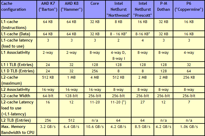
Core gave a 4 MB Level 2 cache between two cores, with a 12-14 cycle access time. This allows each core to use more than 2MB of L2 if needed, something Presler did not allow. Each core also has a 3-cycle 32KB instruction + 32KB data cache, compared to the super small Netburst, and also supports 256 entries in the L1 data TLB, compared to 8. Both the L1 and L2 are accessible by a 256-bit interface, giving good bandwidth to the core.
Note that AMD’s K8 still has a few advantages over Core. The 2-way 64KB L1 caches on AMD’s K8 have a slightly better hit rate to the 8-way 32KB L1 caches on Core, with a similar latency. AMD’s K8 also used an on-die memory controller, lowering memory latency significantly, despite the faster FSB of Intel Core (relative to Netburst) giving a lower latency to Core. As stated in our microarchitecture overview at the time, Athlon 64 X2s memory advantage had gotten smaller, but a key element to the story is that these advantages were negated by other memory sub-system metrics, such as prefetching. Measured by ScienceMark, the Core microarchitecture’s L1 cache delivers 2x bandwidth, and the L2 cache is about 2.5x faster, than the Athlon one.


158 Comments
View All Comments
Hazly79 - Wednesday, July 27, 2016 - link
History of Intel processori 386 1986
i 486 1989 - 94
Pentium / MMX 1994 - 96
Pentium II 1997
Pentium III 1999
Pentium 4 / 4 HT 2002 - 04
Pentium D 2005
Core [ 2 ] Duo 2006 - 08
Core [ 2 ] Quad 2007 - 08
Core [ i ] Nehalem 2008
Core [ i ] Westmere 2009
Core [ i ] Sandy Bridge 2011
Core [ i ] Ivy Bridge 2012
Core [ i ] Haswell 2013
Core [ i ] Broadwell 2014
Core [ i ] Skylake 2015
Core [ i ] Kabylake 2016
AnnonymousCoward - Wednesday, July 27, 2016 - link
So how many decades will it take til cpus have significantly faster single-thread than a 6700K@4.4GHz?Notmyusualid - Thursday, July 28, 2016 - link
+1Mr Perfect - Wednesday, July 27, 2016 - link
Hmm. We've got an ancient 2007 Macbook with a 2GHz C2D(T7200 I think) in it that's still used for web browsing on a daily basis. Upgrading it to 4GB of ram and a SSD made it surprisingly capable.It's not all a bed of roses though, as random things will come out of left field and floor it. I think it's mostly flash heavy sites, but Twitter and Vine freak it out a little.
Hulk - Wednesday, July 27, 2016 - link
I vividly remember the anticipation and hype leading up to the C2D release. The the years of struggle Intel had with Netburst before Conroe. It was what I consider the end of the golden age of the CPU. Great job Ian!Impulseman45 - Wednesday, July 27, 2016 - link
Ah, it wasn't the Pentium Pro it was based on. The Core family was a direct descendant of the Pentium 3 Tualatin. They stopped sales of the of the Pentium 3 Tualatin because it was outperforming the Pentium 4. They migrated that technology to the notebook line as it was much more efficient. It became the Pentium M. When Intel realized that the Pentium 4 Netburst architecture was a dead end and they needed a new chip to go up against AMD, they sourced their notebook chips to build the Core series. See this is what is called re-writing history. Come on guys, it is very well known that they sourced the Pentium M Yohan for the Core series. I do not know who did your research but it is all wrong. Go back and recheck your information. The Pentium Pro was the granddaddy of all the Pentium 2 and 3 chips so yeah, you can point to that chip in a vague way as the ancestor. But the Pentium 4 can as well well. So to be to the point, the core lines DNA goes back directly to the Pentium 3 Tualatin, So we have all been using very, very hopped up Pentium 3s the last 10 years. The Tualatin was an excellent chip. It overclock like crazy. There were Celeron and Sever P3 versions and all of them beat the hell out of the P4. Its know reason Intel had to kill it. Do more research so you can post accurate articles, please.Michael Bay - Thursday, July 28, 2016 - link
>teaching AT about CPU architecturesDamn it, you`re a riot!
Impulseman45 - Thursday, July 28, 2016 - link
These are not the original AT guys, they are all new people and they are not doing the research they should be doing. This is how history can get changed. People look to a reputable tech site that got something wrong and its written in stone. Well AT says this is how it is, even if they are wrong. Go check the history directly from Intel, This article is wrong and that is a fact, period. I felt it just needed to be called out on.natenu - Monday, August 1, 2016 - link
Refreshing to see this comment. HT was a marketing joke to keep up with clock rate shoppers.wumpus - Tuesday, August 2, 2016 - link
When Dave Barry jokes about "speed is measured in Megahertz" you know you are ripe for some marketing in your engineering.