Ten Year Anniversary of Core 2 Duo and Conroe: Moore’s Law is Dead, Long Live Moore’s Law
by Ian Cutress on July 27, 2016 10:30 AM EST- Posted in
- CPUs
- Intel
- Core 2 Duo
- Conroe
- ITRS
- Nostalgia
- Time To Upgrade
Today marks a full 10 years since the first Core 2 Duo processors, and hence Intel’s 64-bit Core microarchitecture, were made officially available at retail. These included a number of popular dual-core processor parts, including the seemingly ubiquitous E6400 and the Core 2 Extreme X6800. These were built on Intel’s 65nm process, and marked a turning point in the desktop processor ecosystem. To quote Anand in our launch review: ‘you’re looking at the most impressive piece of silicon the world has ever seen’.
Ten Year Anniversary of Core 2 Duo and Conroe
As part of this piece we will also look at some of the predictions for the future, from the latest (and possibly last) International Technology Roadmap for Semiconductors report, which predicts the stalling of smaller silicon manufacturing nodes over the next 10-15 years.
The first part of this article borrows heavily from Johan’s original look into the Intel Core microarchitecture back in 2006. It’s an awesome read.
Back When I Were A Lad
For a number of our readers, the launch of Conroe was a vast change in the processing landscape. The family of Netburst, Northwood and Prescott processors, in the form of Pentium D and Pentium 4, showed that pursuing the frequency race pushed the silicon far outside its efficiency zone and left a hot, power hungry mess in its wake. It didn’t even come with a muscular V8 sound, and AMD’s Athlon 64 X2 line had taken both the performance and efficiency crown.
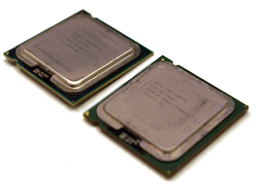
Core 2 Duo (left) vs Pentium D (right)
From the perspective of Intel, it had to incorporate a significant paradigm shift in the way it approached the core microarchitecture – no more long pipelines to bump up clock rates to start. The Core microarchitecture design was marketed as a blend of Pentium Pro and Pentium M techniques, as well as the Netburst architecture, however as Johan pointed out at the time, it is significantly Pentium M and it is very hard to find anything Netburst in there. It wasn’t as simple as ‘adding a few functional units or decoders on Yonah and calling it a day’, almost 80% of the architecture and circuit design had to be redone.
As part of this piece, we’re going to take another look at the original architecture improvements of the Core microarchitecture design and some of our old performance metrics from a decade ago.
27th July 2006: Core 2 Launch Day
Ten years ago, Intel launched the following five processors:
| CPU | Clock Speed | L2 Cache |
| Intel Core 2 Extreme X6800 | 2.93GHz | 4MB |
| Intel Core 2 Duo E6700 | 2.66GHz | 4MB |
| Intel Core 2 Duo E6600 | 2.40GHz | 4MB |
| Intel Core 2 Duo E6400 | 2.13GHz | 2MB |
| Intel Core 2 Duo E6300 | 1.86GHz | 2MB |
The X6800 sits at the top with a higher clock speed with a higher supported FSB-to-core ration than previous Intel processors. The Core 2 processors all came from a 143mm2 die, compared the 162mm2 of Pentium D, and they both seem tiny by comparison to the large die sizes we see 2016 for things like the P100. These were chips without integrated graphics either. The introduction of Core 2 pushed the prices of the Pentium D processors down, to give this interesting table:
| CPU | Clock Speed | L2 Cache | Price |
| Intel Core 2 Extreme X6800 | 2.93GHz | 4MB | $999 |
| Intel Core 2 Duo E6700 | 2.66GHz | 4MB | $530 |
| Intel Core 2 Duo E6600 | 2.40GHz | 4MB | $316 |
| Intel Core 2 Duo E6400 | 2.13GHz | 2MB | $224 |
| Intel Core 2 Duo E6300 | 1.86GHz | 2MB | $183 |
| Intel Pentium D 945 | 3.40GHz | 2MBx2 | $163 |
| Intel Pentium D 915 | 2.80GHz | 2MBx2 | $133 |
| Intel Pentium D 820 | 2.80GHz | 1MBx2 | $113 |
| Intel Pentium D 805 | 2.66GHz | 1MBx2 | $93 |
Comparing this to recent Intel processors, and the X8600 matches the list price of the Core i7-5960X (an 8-core part), whereas the popular Core 2 Duo E6400 at $224 at the same price as the Core i5-6600.
A few years ago, I salvaged a super old computer of mine with an E6400 and took it for a spin for a pipeline piece entitled ‘Dragging Core 2 Duo into 2013’. We know that a number of users today are still using the old platform as their day to day machine, and given that it is now celebrating its 10th birthday, it is interesting that anyone wanting to play around with the old hardware can get a motherboard, memory and CPU from eBay for $50-70.
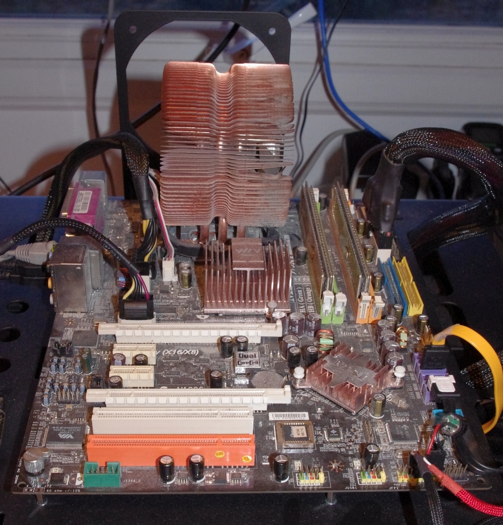
My crusty C2D Setup from 2013


158 Comments
View All Comments
Hazly79 - Wednesday, July 27, 2016 - link
History of Intel processori 386 1986
i 486 1989 - 94
Pentium / MMX 1994 - 96
Pentium II 1997
Pentium III 1999
Pentium 4 / 4 HT 2002 - 04
Pentium D 2005
Core [ 2 ] Duo 2006 - 08
Core [ 2 ] Quad 2007 - 08
Core [ i ] Nehalem 2008
Core [ i ] Westmere 2009
Core [ i ] Sandy Bridge 2011
Core [ i ] Ivy Bridge 2012
Core [ i ] Haswell 2013
Core [ i ] Broadwell 2014
Core [ i ] Skylake 2015
Core [ i ] Kabylake 2016
AnnonymousCoward - Wednesday, July 27, 2016 - link
So how many decades will it take til cpus have significantly faster single-thread than a 6700K@4.4GHz?Notmyusualid - Thursday, July 28, 2016 - link
+1Mr Perfect - Wednesday, July 27, 2016 - link
Hmm. We've got an ancient 2007 Macbook with a 2GHz C2D(T7200 I think) in it that's still used for web browsing on a daily basis. Upgrading it to 4GB of ram and a SSD made it surprisingly capable.It's not all a bed of roses though, as random things will come out of left field and floor it. I think it's mostly flash heavy sites, but Twitter and Vine freak it out a little.
Hulk - Wednesday, July 27, 2016 - link
I vividly remember the anticipation and hype leading up to the C2D release. The the years of struggle Intel had with Netburst before Conroe. It was what I consider the end of the golden age of the CPU. Great job Ian!Impulseman45 - Wednesday, July 27, 2016 - link
Ah, it wasn't the Pentium Pro it was based on. The Core family was a direct descendant of the Pentium 3 Tualatin. They stopped sales of the of the Pentium 3 Tualatin because it was outperforming the Pentium 4. They migrated that technology to the notebook line as it was much more efficient. It became the Pentium M. When Intel realized that the Pentium 4 Netburst architecture was a dead end and they needed a new chip to go up against AMD, they sourced their notebook chips to build the Core series. See this is what is called re-writing history. Come on guys, it is very well known that they sourced the Pentium M Yohan for the Core series. I do not know who did your research but it is all wrong. Go back and recheck your information. The Pentium Pro was the granddaddy of all the Pentium 2 and 3 chips so yeah, you can point to that chip in a vague way as the ancestor. But the Pentium 4 can as well well. So to be to the point, the core lines DNA goes back directly to the Pentium 3 Tualatin, So we have all been using very, very hopped up Pentium 3s the last 10 years. The Tualatin was an excellent chip. It overclock like crazy. There were Celeron and Sever P3 versions and all of them beat the hell out of the P4. Its know reason Intel had to kill it. Do more research so you can post accurate articles, please.Michael Bay - Thursday, July 28, 2016 - link
>teaching AT about CPU architecturesDamn it, you`re a riot!
Impulseman45 - Thursday, July 28, 2016 - link
These are not the original AT guys, they are all new people and they are not doing the research they should be doing. This is how history can get changed. People look to a reputable tech site that got something wrong and its written in stone. Well AT says this is how it is, even if they are wrong. Go check the history directly from Intel, This article is wrong and that is a fact, period. I felt it just needed to be called out on.natenu - Monday, August 1, 2016 - link
Refreshing to see this comment. HT was a marketing joke to keep up with clock rate shoppers.wumpus - Tuesday, August 2, 2016 - link
When Dave Barry jokes about "speed is measured in Megahertz" you know you are ripe for some marketing in your engineering.