ARM Unveils Next Generation Bifrost GPU Architecture & Mali-G71: The New High-End Mali
by Ryan Smith on May 30, 2016 7:00 AM ESTThe Bifrost Quad: Replacing ILP with TLP
The solution then, as the echo of GPU development catches up with mobile, is to make the move to a scalar, Thread Level Parallelism-centric architecture. And this is exactly the direction ARM is going with Bifrost.
Continuing ARM’s theme of Norse-named architectures, Bifrost is a distinctly TLP-centric (though not TLP-exclusive) architecture. In designing Bifrost, ARM’s GPU group likes to joke that they just turned their old shader core 90° to the left, which all things considered is not a bad analogy. Rather than trying to extract 4 instruction’s worth of ILP from a single thread, ARM groups 4 threads together and executes a single instruction from each one.
If all of this sounds familiar to our long-time readers, then it should. This is a very similar transition to what AMD made with Graphics Core Next in 2011, a move that significantly improved AMD’s GPU throughput and suitability for modern rendering paradigms. And for ARM we are going to see a lot of the same.
The simply beauty of a TLP-centric design is that it doesn’t require making extensive efforts to extract instruction level parallelism from a thread. Graphics rendering itself is an embarrassingly parallel problem, and the increase in screen resolutions over the years has further increased the number of pixels (and therefore threads) that need processed. Thus by nearly eliminating a reliance on ILP, ARM is able to much more easily achieve full utilization of its shader core.
The benefit for ARM here is twofold. In the case of graphics, a TLP-centric design improves utilization, especially with newer rendering paradigms that only operate on one or two components at a time. However increasingly important is the fact that TLP designs are also much more compute friendly, and this is an important distinction for ARM as solid GPU compute performance becomes an increasingly component of modern mobile devices.
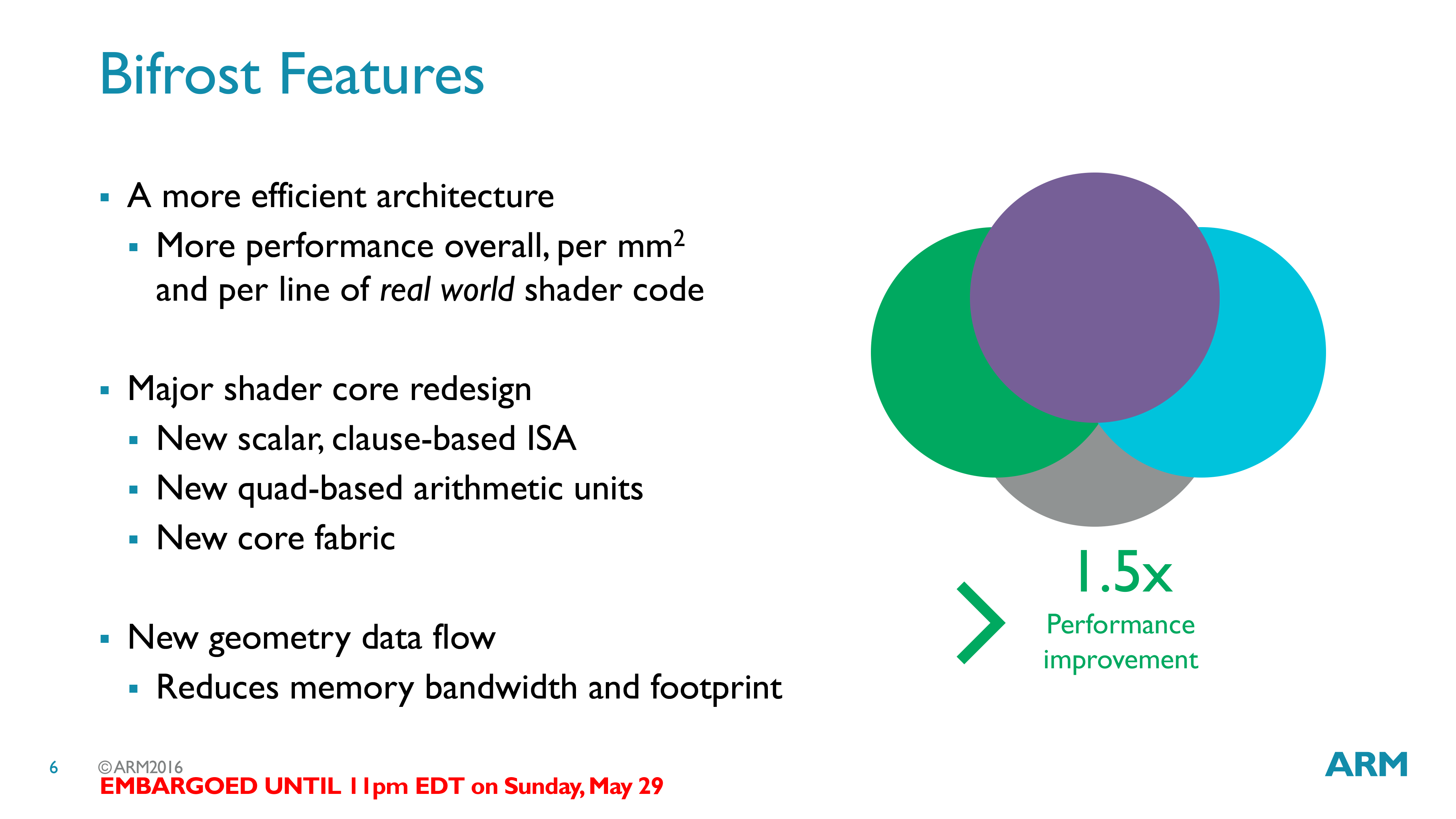
This increase in utilization also has an impact on power consumption, and ultimately area efficiency. In conjunction with architectural improvements made elsewhere, Bifrost’s higher average utilization means the design should have better performance per mm2 of die space, which is an important metric for the market ARM serves. The company’s architectural update also brings with it certain side benefits to aspects such as bandwidth needs for the L1 instruction cache, which allows for a lower power data path between the cache and shader core.
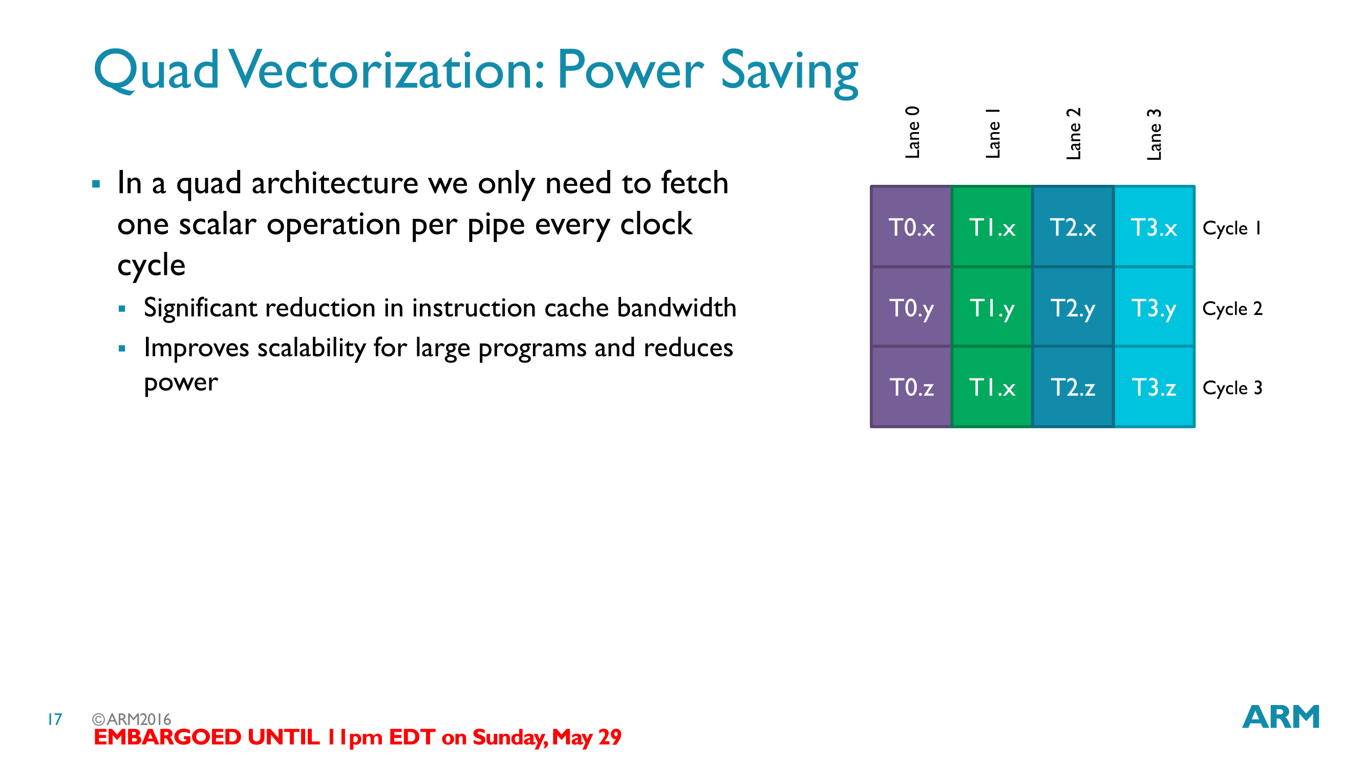
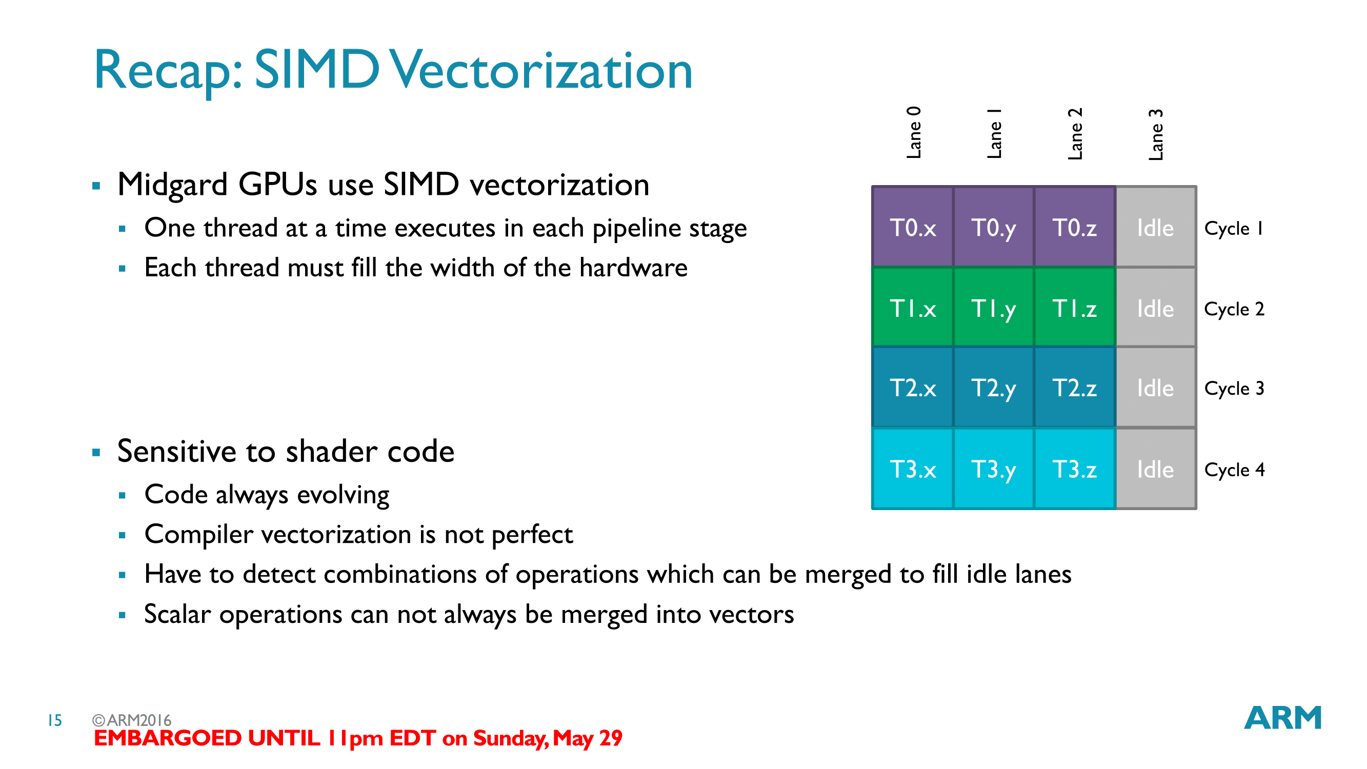
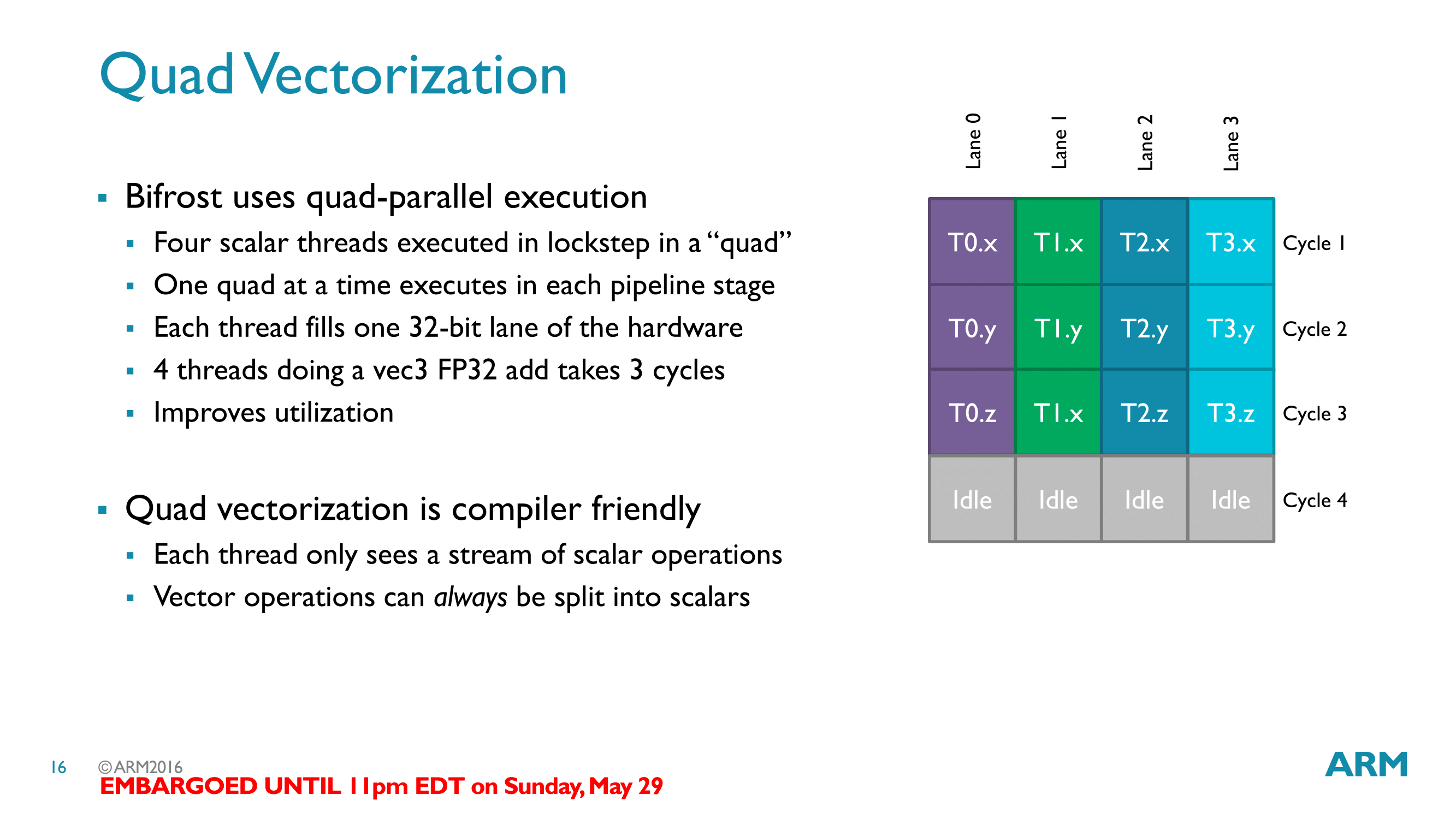
Moving on, within the Bifrost architecture, ARM’s wavefronts are called Quads. True to the name, these are natively 4 threads wide, and a row of instructions from a full quad is executed per clock cycle. Bifrost’s wavefront size is particularly interesting here, as quads are much smaller than competing architectures, which are typically in the 16-32 thread range. Wavefront design in general reflects the need to find a balance between resource/area density and performance. Wide wavefronts require less control logic (ex: 32 threads with 1 unit of control logic, versus 4x8 threads with 8 units of control logic), but at the same time the wider the wavefront, the harder it is to fill.
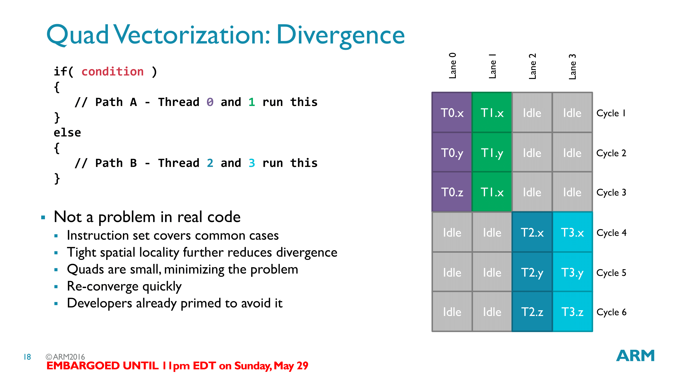
ARM’s GPU philosophy in general has been concerned with trying to avoid execution stalls, and their choice in wavefront size reflects this. By going with a narrower wavefront, a group of threads is less likely to diverge – that is, take different paths, typically as a result of a conditional statement – than a wider wavefront. Divergences are easy enough to handle (just follow both paths), but the split hurts performance.
Diving a bit deeper, let’s take a look at the individual arithmetic pipelines inside of a quad execution engine. In Midgard, ARM’s pipelines contained vector units for vector addition, vector multiplication, vector Special Functions Unit (SFU) scalar addition, and scalar multiplication. Bifrost on the other hand simplifies this. With Bifrost a pipeline is just a 128bit (4x32bit) FMA SIMD, and then a second 128bit SIMD for interger addition and SFU operations. Each 32bit slot is in turn filled with an instruction from its respective thread in the quad.
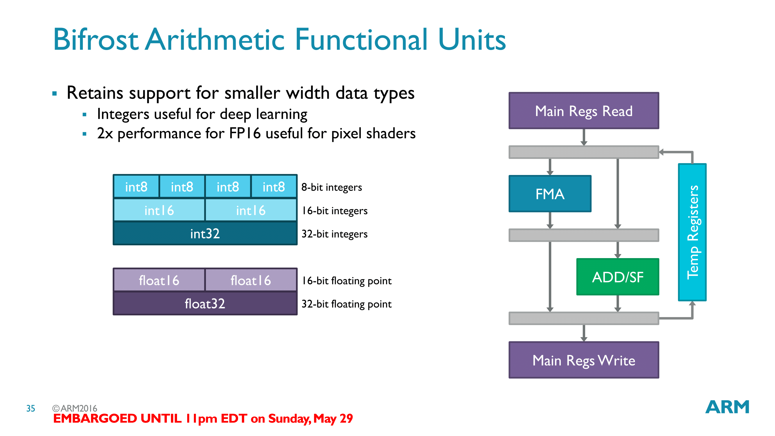
That interger additions and special functions are together on the same SIMD (FP adds are done on the FMA unit) is a unique hallmark of Bifrost, as most other architectures put all addition and multiplication down the same pipe. On the other hand it means that, just like Midgard, ARM can execute a multiplication/FMA and a separate add at the same time. This is also why Bifrost is not a TLP-exclusive design. Technically ARM is issuing a fused instruction, the Slightly Long Instruction Word, which is composed of separate instructions for the FMA and ADD/SFU SIMDs. Consequently to get maximum utilization of the GPU, both SIMDs need to be filled. However with that said, the traditional definitions usually involve just FMAs, so how much this is really reliant on ILP compared to other architectures is up to debate.
Meanwhile within the SIMDs, ARM has confirmed that like with Midgard, Bifrost is capable of instruction decomposition/fusion, meaning that a single SIMD lane can be packed with different data types. For floating point operations one lane can handle 1 FP32 or 2 FP16 per clock, and for integer operations this is 1 INT32, 2 INT16s, or 4 INT8s per clock. This continues to be a differentiating feature of ARM’s GPU architectures as compared to some other designs, as they maintain the single ALU whereas some other vendors use dedicated FP32 and FP16 ALUs, trading between space and power efficiency.
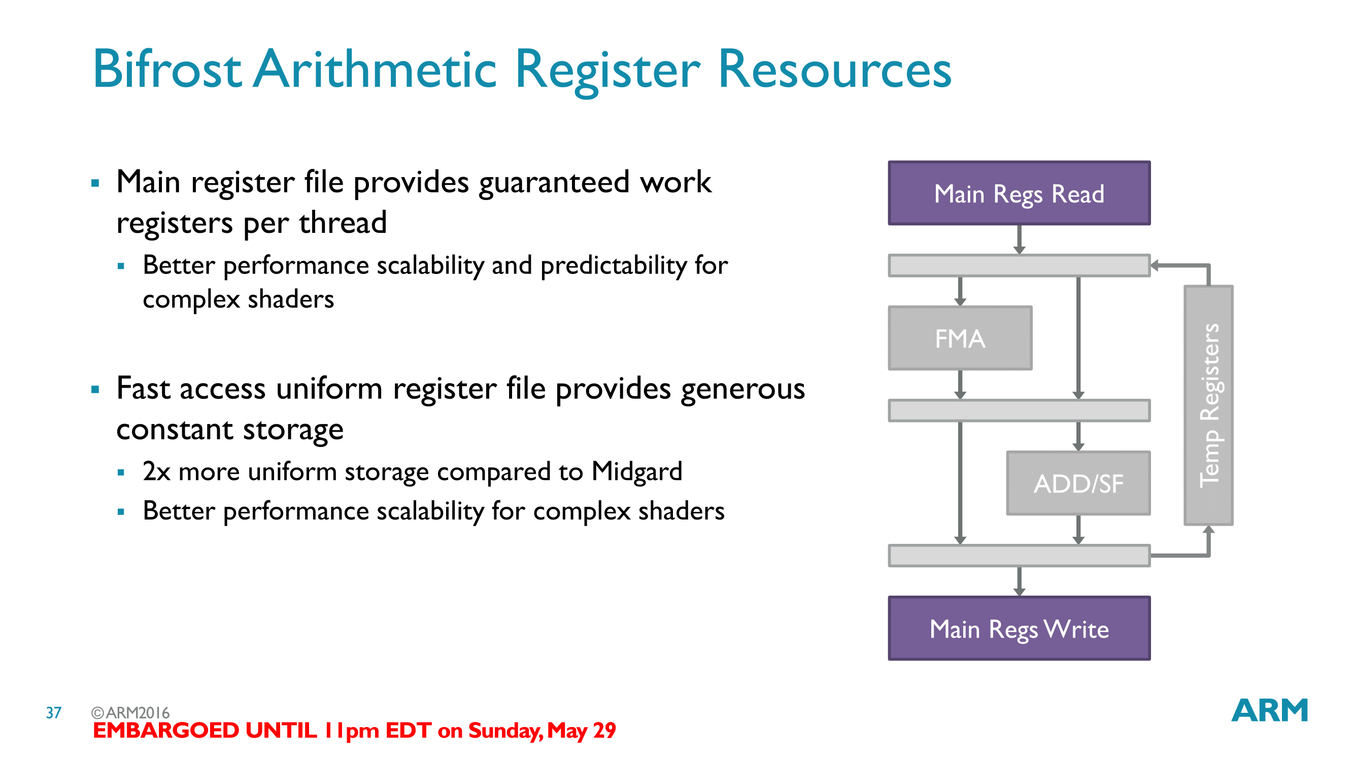
ARM has also confirmed that the register file within each pipeline has been enlarged relative to Midgard. Though a specific size wasn’t specified, Bifrost’s register file size is twice that of Midgard’s. ARM specifically cites this as being important for improving the architecture’s ability to handle long, complex shaders that may have overflowed the register file on Midgard.
Going back up a level, before getting into a high level overview of Bifrost, let’s talk a bit about how ARM is actually scheduling threads for Bifrost. Along with the reorganization of their shader core into the quad, ARM has also added support for an interesting feature called clauses. Clauses, in a nutshell, are a type of wavefront with restrictions. The idea behind a clause being that by defining additional requirements about how instructions are ordered, and identifying instructions with variable latency, ARM can cut down on instruction scheduling overhead.

When a wavefront is organized into a clause by the compiler, the instructions within that wavefront are given certain execution guarantees. The latency for all instructions is known and they are executed back to back to the end of the clause. In essence a clause is a block of instructions the compiler knows is absolutely safe to run from start to finish without checking in on it.
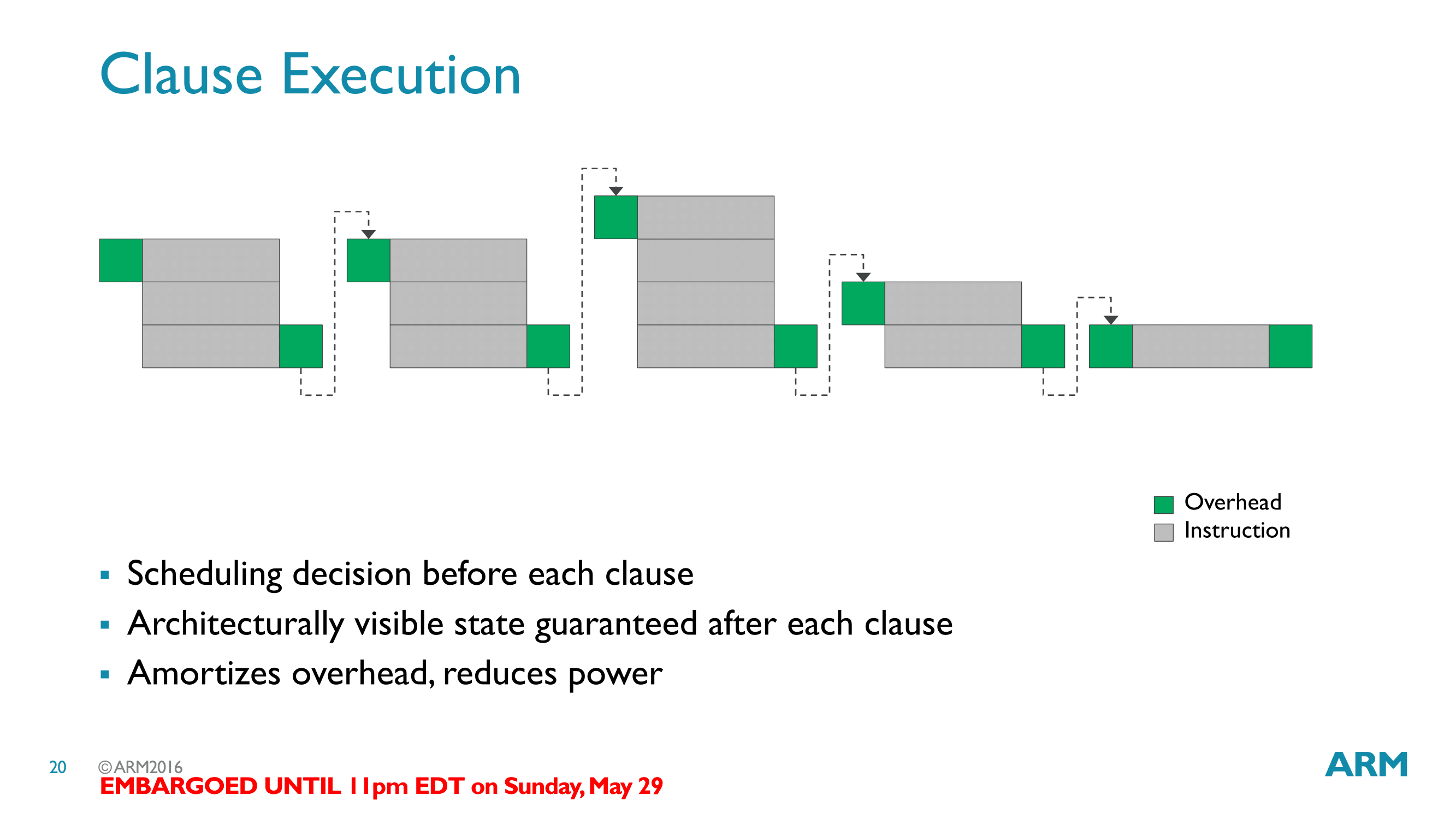
The payoff for using clauses is that because clauses have execution guarantees, the GPU scheduler can avoid the overhead of checking on a quad execution engine as frequently, only returning to check on it after the clause is done. This overhead reduction then is captured as power savings.
But the benefits to Bifrost from clauses don’t stop there. When executing clauses, Bifrost can chain together instructions that would need to access the same register back-to-back, and in some cases bypass that register access. Register file accesses are relatively expensive from a power standpoint, so avoiding using the register file is another means to save power, and ultimately it allows ARM to get away with a simpler register file.
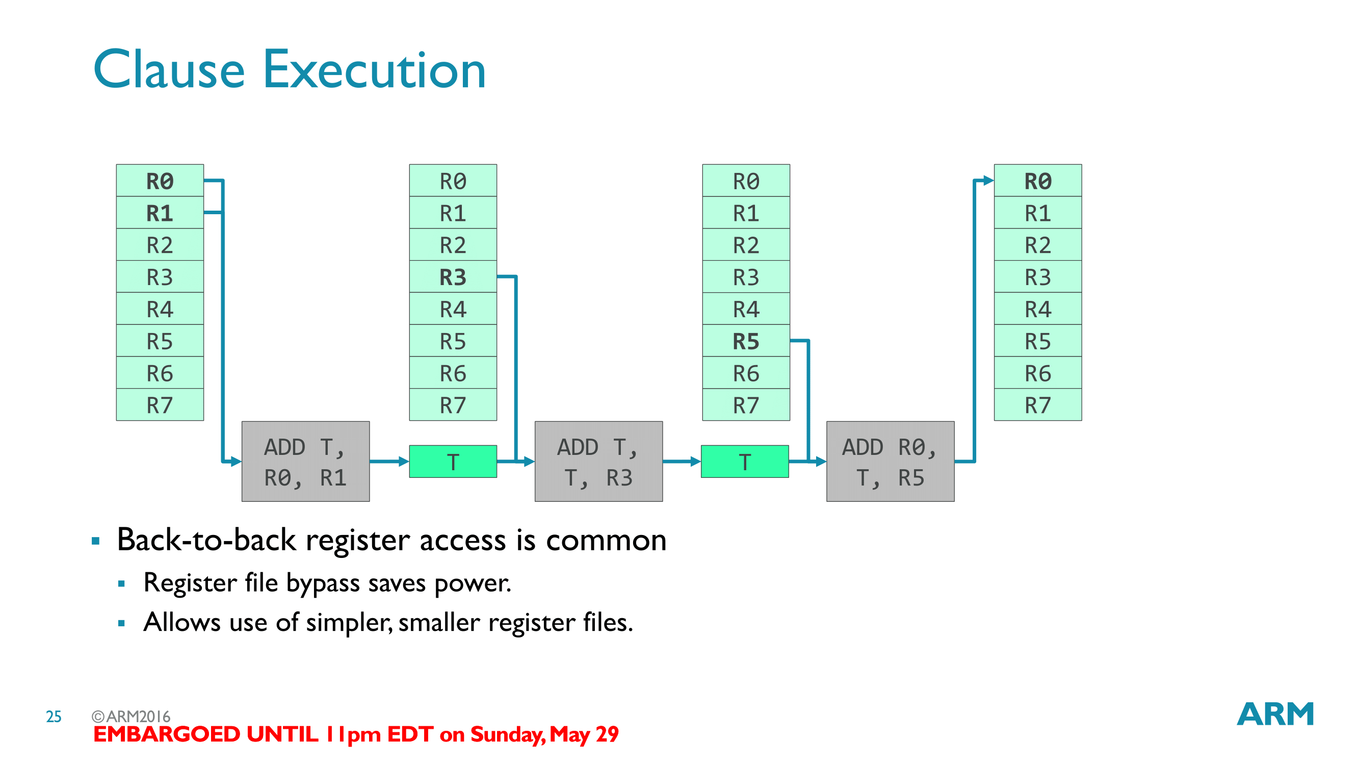
ARM calls this implementation a temporary register, and while it’s more of a mental mnemonic than a true register, the basic idea is that the result of an instruction is immediately fed into the input of the next instruction. The nature of this data feeding means that it can only take place within a clause, as the result will only be available for a single cycle. This in turn is why the temporary register really is temporary; the data has to be used next cycle or it would be lost.
Finally, ARM has also illustrated how clauses work with respect to variable latency instructions, such as texture accesses. Variable latency operations are allowed in a clause, but only at the boundaries of a clause. In essence a variable latency operation splits a clause into two parts, with the access marking the end of a clause and the operation using the resource accessed marking the start of another clause.
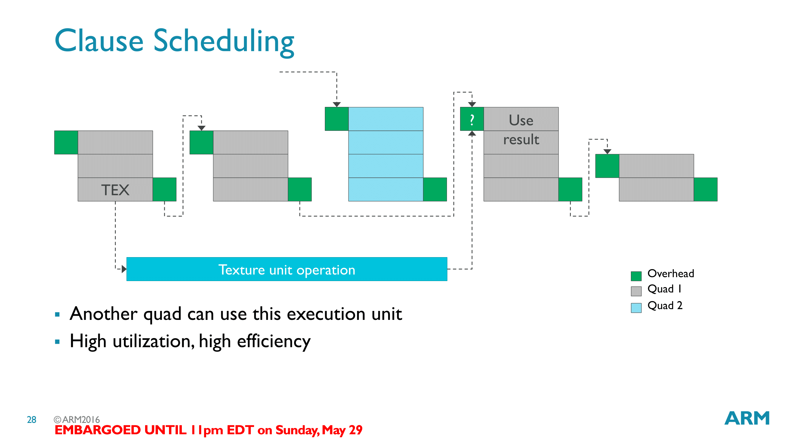
By splitting clauses in this manner, ARM is able to schedule clauses around these variable latency operations. When the second half of a clause is not ready to begin, another, unrelated clause can be interleaved into the quad. Interleaving clauses is a textbook solution to latency hiding, as it allows the quads to stay active with other work while waiting on high latency operations, with each clause/wavefront covering for the latency of the others. In the case of ARM, Bifrost just takes it one step further due to the introduction of clauses, more strictly defining when interleaving takes place. Overall ARM can interleave up to 8 such streams of clauses.


57 Comments
View All Comments
Shadow7037932 - Tuesday, May 31, 2016 - link
Mobile VR (hopefully, meaning "cheaper" VR) for starters.Spunjji - Wednesday, June 1, 2016 - link
Your lack of imagination is staggering.Zyzzyx - Wednesday, June 1, 2016 - link
This technology is going to affect millions if not billions of customers over the next few years, your 1080 will be used by a limited number of gamers, we know already about the Pascal architecture, as it has already been covered. Claiming that mobile dGPUs have no importance sounds like Ballmer saying the iphone had no market.You might also have missed the iPad Pro and what you can use it for, and no it is not mobile gaming ...
Also your claim that only Windows 10 is a real OS shows your short sightedness, we will see in 5-10 years which OS will be dominating, since i am sure both Android and iOS will slowly but surely keep creeping into the professional space as features will be added.
Wolfpup - Friday, June 3, 2016 - link
You sound like me LOL. Still interesting though just on a tech level, but I use PCs and game systems as they have actual games (and good interfaces to play them).SolvalouLP - Monday, May 30, 2016 - link
We all are waiting for AT review of GTX 1080, but please, this behaviour is childish at best.Ryan Smith - Monday, May 30, 2016 - link
And your hope will be rewarded.makerofthegames - Tuesday, May 31, 2016 - link
Go ahead and take as long as you need. I don't read AT for the hot takes, I read AT because you do real testing and real analysis to give us real information. I definitely want to read the review, but I'm willing to wait for it to be good.edlee - Monday, May 30, 2016 - link
It all sounds great, unfortunately I am stuck with devices that get powered by qualcomm sons, since I have verizon, and most flagship phone use qualcomm snapdragonsKrysto - Monday, May 30, 2016 - link
It's a shame Samsung isn't selling its Exynos chip to other device makers, isn't it? I mean, it's probably not even economically worth it for Samsung to design a chip for only 1 or 2 of its smartphone models. I don't understand why they don't try to compete more directly with Qualcomm in the chip market. I also don't understand why they aren't buying AMD so they can compete more directly with Intel as well, but I digress.Tabalan - Monday, May 30, 2016 - link
Samsung sells certain Exynos SoC to Meizu, Meizu MX4 Pro had Exynos 5430, Pro 5 had Exynos 7420. With Pro 6 they went Mediatek X25.About costs of designing and profit - they used to use CPU core and GPU designed by ARM, it's cheaper this way than buying license to modify these cores (and you have to add R&D costs of modifying uarch). Moreover, Samsung is using their latest process node only for high end SoCs (Apple AX series, Snapdragon 8XX series), which is very profitable market share. It could be easier to just manufacture SoC and get cash for it than looking for partners, vendees for their SoC. Plus, they would have to create whole line up of Exynos SoC to compete with Qualcomm (I assume Qc would give discount for buying chips only from them).