The NVIDIA GeForce GTX 1080 & GTX 1070 Founders Editions Review: Kicking Off the FinFET Generation
by Ryan Smith on July 20, 2016 8:45 AM ESTGP104: The Heart of GTX 1080
At the heart of the GTX 1080 is the first of the consumer-focused Pascal GPUs, GP104. Though no two GPU generations are ever quite alike, GP104 follows a number of design cues established with the past couple 104 GPUs. Overall 104 GPUs have struck a balance between size and performance, allowing NVIDIA to get a suitably high yielding GPU out at the start of a generation, and to be followed up with larger GPUs later on as yields improve. With the exception of the GTX 780, 104 GPUs been the backbone of NVIDIA’s GTX 70 and 80 parts, and that is once again the case for the Pascal generation.
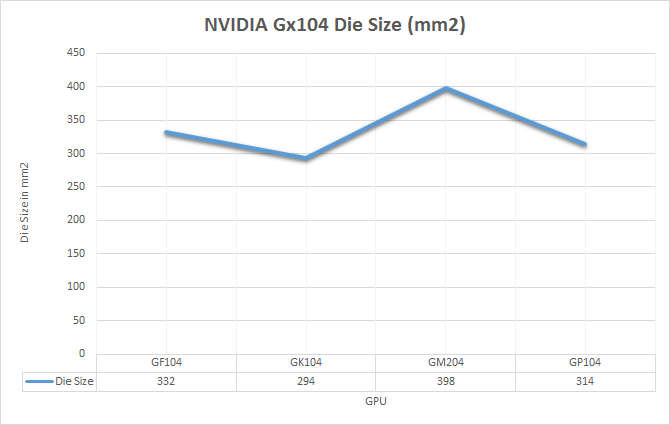
In terms of die size, GP104 comes in at 314mm2. This is right in NVIDIA’s traditional sweet spot for these designs, slotting in between the 294mm2 GK104 and the 332mm2 GF104. In terms of total transistors we’re looking at 7.2B transistors, up from 3.5B on GK104 and the 5.2B of the more unusual GM204. The significant increase in density comes from the use of TSMC’s 16nm FinFET process, which compared to 28nm combines a full node shrink, something that has been harder and harder to come by as the years have progressed.
Though the density improvement offered by TSMC’s 16nm process is of great importance to GP104’s overall performance, for once density takes a back seat to the properties of the process itself. I am of course speaking about the FinFET transistors, which are the headlining feature of TSMC’s process.
We’ve covered FinFET technology in depth before, so I won’t completely rehash it here. But in brief, FinFETs are an important development for chip fabrication as processes have gone below 28nm. As traditional, planar transistors have shrunk in feature size – and ultimately, the number of atoms they’re comprised of – electrical leakage has increased. With fewer atoms in a transistor, there are equally fewer atoms to control the flow of electrons.
FinFET in turn is a solution to this problem, essentially allowing fabs to turn back the clock on electrical leakage. By building transistors as three-dimensional objects with height as opposed to two-dimensional objects, giving FinFET transistors their characteristic fins in the process, FinFET technology greatly reduces the amount of energy a transistor leaks. In practice what this means is that FinFET technology not only reduces the total amount of energy wasted from leakage, but it also allows transistors to be operated at a much lower voltage, something we’ll see in depth with our analysis of GTX 1080.
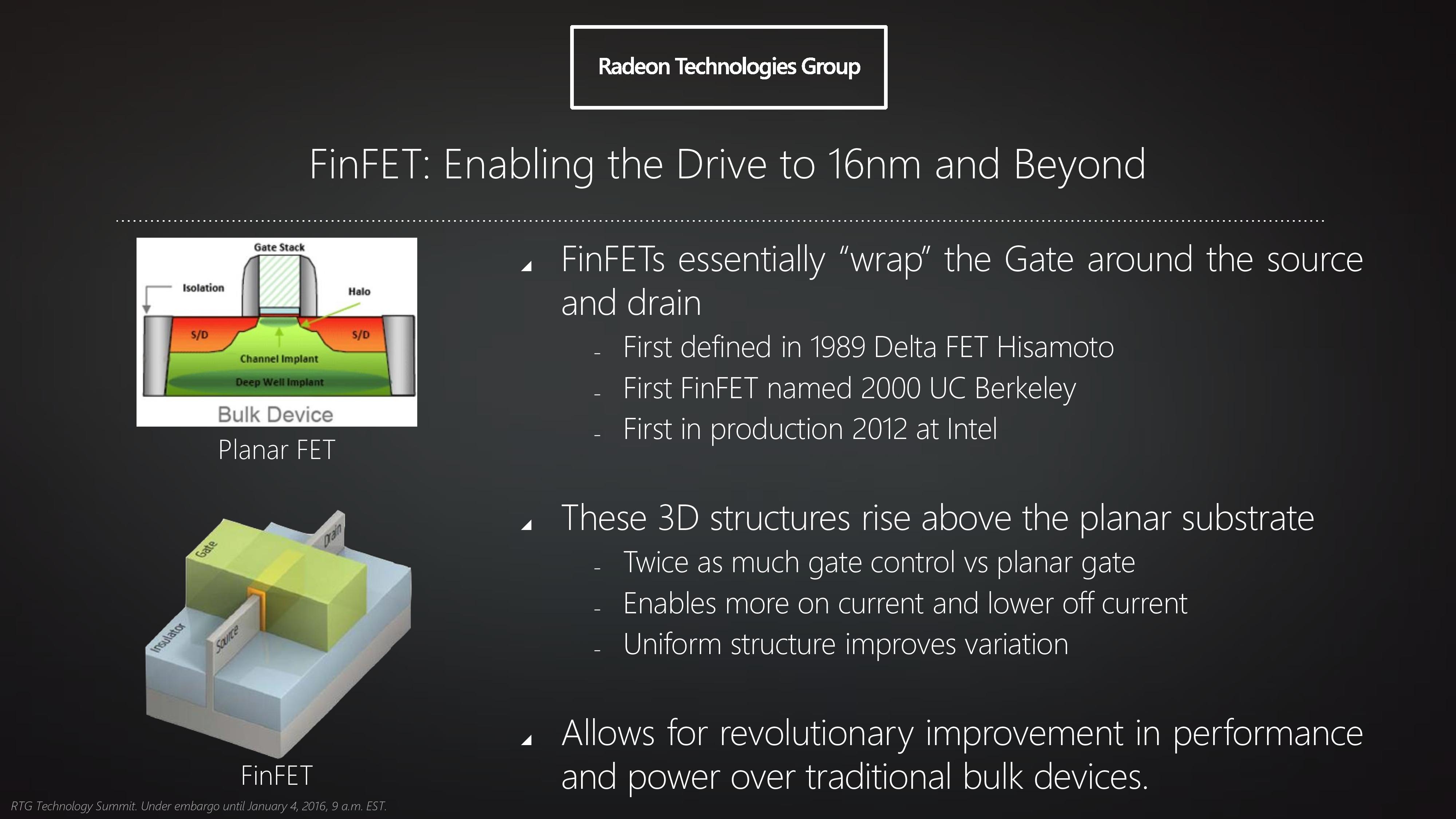
FinFETs, or rather the lack thereof, are a big part of why we never saw GPUs built on TSMC’s 20nm process. It was TSMC’s initial belief that they could contain leakage well enough using traditional High-K Metal Gate (HKMG) technology on 20nm, a bet they ultimately lost. At 20nm, planar transistors were just too leaky to use for many applications, which is why ultimately we only saw SoCs on 20nm (and even then they were suboptimal). FinFETs, as it turns out, are absolutely necessary to get good performance out of transistors built on processes below 28nm.
And while it took TSMC some time to get there, now that they have the capability NVIDIA can reap the benefits. Not only can NVIDIA finally build a relatively massive chip like a GPU on a sub-28nm process, but thanks to the various beneficial properties of FinFETs, it allows them to take their designs in a different direction than what they could do on 28nm.


200 Comments
View All Comments
TestKing123 - Wednesday, July 20, 2016 - link
Then you're woefully behind the times since other sites can do this better. If you're not able to re-run a benchmark for a game with a pretty significant patch like Tomb Raider, or a high profile game like Doom with a significant performance patch like Vulcan that's been out for over a week, then you're workflow is flawed and this site won't stand a chance against the other crop. I'm pretty sure you're seeing this already if you have any sort of metrics tracking in place.TheinsanegamerN - Wednesday, July 20, 2016 - link
So question, if you started this article on may 14th, was their no time in the over 2 months to add one game to that benchmark list?nathanddrews - Wednesday, July 20, 2016 - link
Seems like an official addendum is necessary at some point. Doom on Vulkan is amazing. Dota 2 on Vulkan is great, too (and would be useful in reviews of low end to mainstream GPUs especially). Talos... not so much.Eden-K121D - Thursday, July 21, 2016 - link
Talos Principle was a proof of conceptajlueke - Friday, July 22, 2016 - link
http://www.pcgamer.com/doom-benchmarks-return-vulk...Addendum complete.
mczak - Wednesday, July 20, 2016 - link
The table with the native FP throughput rates isn't correct on page 5. Either it's in terms of flops, then gp104 fp16 would be 1:64. Or it's in terms of hw instruction throughput - then gp100 would be 1:1. (Interestingly, the sandra numbers for half-float are indeed 1:128 - suggesting it didn't make any use of fp16 packing at all.)Ryan Smith - Wednesday, July 20, 2016 - link
Ahh, right you are. I was going for the FLOPs rate, but wrote down the wrong value. Thanks!As for the Sandra numbers, they're not super precise. But it's an obvious indication of what's going on under the hood. When the same CUDA 7.5 code path gives you wildly different results on Pascal, then you know something has changed...
BurntMyBacon - Thursday, July 21, 2016 - link
Did nVidia somehow limit the ability to promote FP16 operations to FP32? If not, I don't see the point in creating such a slow performing FP16 mode in the first place. Why waste die space when an intelligent designer can just promote the commands to get normal speeds out of the chip anyways? Sure you miss out on speed doubling through packing, but that is still much better than the 1/128 (1/64) rate you get using the provided FP16 mode.Scali - Thursday, July 21, 2016 - link
I think they can just do that in the shader compiler. Any FP16 operation gets replaced by an FP32 one.Only reading from buffers and writing to buffers with FP16 content should remain FP16. Then again, if their driver is smart enough, it can even promote all buffers to FP32 as well (as long as the GPU is the only one accessing the data, the actual representation doesn't matter. Only when the CPU also accesses the data, does it actually need to be FP16).
owan - Wednesday, July 20, 2016 - link
Only 2 months late and published the day after a different major GPU release. What happened to this place?