The NVIDIA GeForce GTX 1080 & GTX 1070 Founders Editions Review: Kicking Off the FinFET Generation
by Ryan Smith on July 20, 2016 8:45 AM ESTGP104: The Heart of GTX 1080
At the heart of the GTX 1080 is the first of the consumer-focused Pascal GPUs, GP104. Though no two GPU generations are ever quite alike, GP104 follows a number of design cues established with the past couple 104 GPUs. Overall 104 GPUs have struck a balance between size and performance, allowing NVIDIA to get a suitably high yielding GPU out at the start of a generation, and to be followed up with larger GPUs later on as yields improve. With the exception of the GTX 780, 104 GPUs been the backbone of NVIDIA’s GTX 70 and 80 parts, and that is once again the case for the Pascal generation.
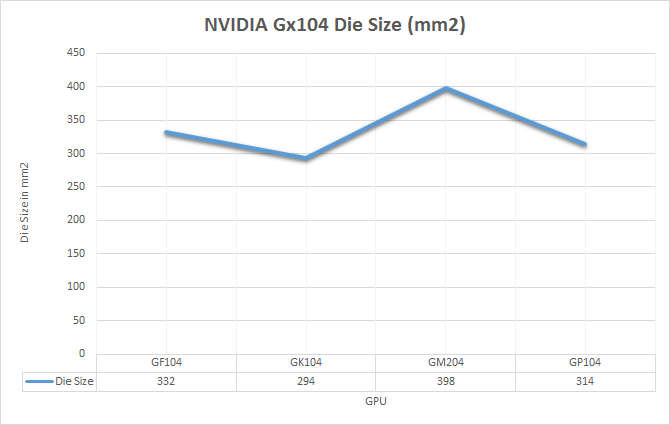
In terms of die size, GP104 comes in at 314mm2. This is right in NVIDIA’s traditional sweet spot for these designs, slotting in between the 294mm2 GK104 and the 332mm2 GF104. In terms of total transistors we’re looking at 7.2B transistors, up from 3.5B on GK104 and the 5.2B of the more unusual GM204. The significant increase in density comes from the use of TSMC’s 16nm FinFET process, which compared to 28nm combines a full node shrink, something that has been harder and harder to come by as the years have progressed.
Though the density improvement offered by TSMC’s 16nm process is of great importance to GP104’s overall performance, for once density takes a back seat to the properties of the process itself. I am of course speaking about the FinFET transistors, which are the headlining feature of TSMC’s process.
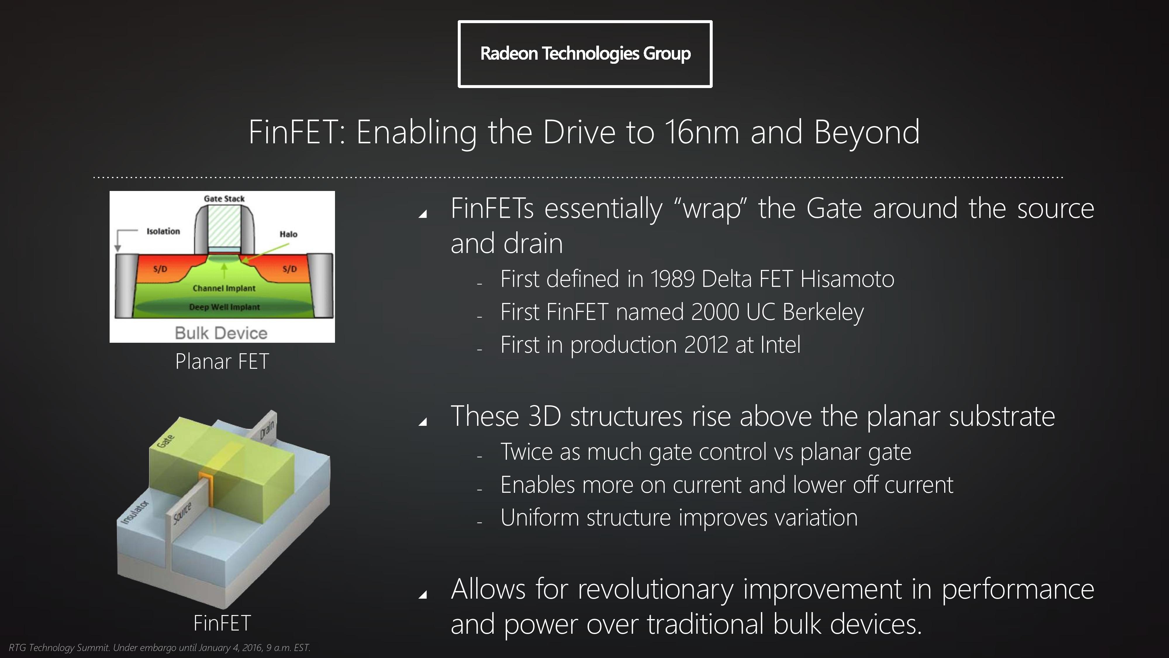
We’ve covered FinFET technology in depth before, so I won’t completely rehash it here. But in brief, FinFETs are an important development for chip fabrication as processes have gone below 28nm. As traditional, planar transistors have shrunk in feature size – and ultimately, the number of atoms they’re comprised of – electrical leakage has increased. With fewer atoms in a transistor, there are equally fewer atoms to control the flow of electrons.
FinFET in turn is a solution to this problem, essentially allowing fabs to turn back the clock on electrical leakage. By building transistors as three-dimensional objects with height as opposed to two-dimensional objects, giving FinFET transistors their characteristic fins in the process, FinFET technology greatly reduces the amount of energy a transistor leaks. In practice what this means is that FinFET technology not only reduces the total amount of energy wasted from leakage, but it also allows transistors to be operated at a much lower voltage, something we’ll see in depth with our analysis of GTX 1080.
FinFETs, or rather the lack thereof, are a big part of why we never saw GPUs built on TSMC’s 20nm process. It was TSMC’s initial belief that they could contain leakage well enough using traditional High-K Metal Gate (HKMG) technology on 20nm, a bet they ultimately lost. At 20nm, planar transistors were just too leaky to use for many applications, which is why ultimately we only saw SoCs on 20nm (and even then they were suboptimal). FinFETs, as it turns out, are absolutely necessary to get good performance out of transistors built on processes below 28nm.
And while it took TSMC some time to get there, now that they have the capability NVIDIA can reap the benefits. Not only can NVIDIA finally build a relatively massive chip like a GPU on a sub-28nm process, but thanks to the various beneficial properties of FinFETs, it allows them to take their designs in a different direction than what they could do on 28nm.


200 Comments
View All Comments
Ryan Smith - Wednesday, July 20, 2016 - link
Thanks.Eden-K121D - Wednesday, July 20, 2016 - link
Finally the GTX 1080 reviewguidryp - Wednesday, July 20, 2016 - link
This echoes what I have been saying about this generation. It is really all about clock speed increases. IPC is essentially the same.This is where AMD lost out. Possibly in part the issue was going with GloFo instead of TSMC like NVidia.
Maybe AMD will move Vega to TSMC...
nathanddrews - Wednesday, July 20, 2016 - link
Curious... how did AMD lose out? Have you seen Vega benchmarks?TheinsanegamerN - Wednesday, July 20, 2016 - link
its all about clock speed for Nvidia, but not for AMD. AMD focused more on ICP, according to them.tarqsharq - Wednesday, July 20, 2016 - link
It feels a lot like the P4 vs Athlon XP days almost.stereopticon - Wednesday, July 20, 2016 - link
My favorite era of being a nerd!!! Poppin' opterons into s939 and pumpin the OC the athlon FX levels for a fraction of the price all while stompin' on pentium. It was a good (although expensive) time to a be a nerd... Besides paying 100 dollars for 1gb of DDR500. 6800gs budget friendly cards, and ATi x1800/1900 super beasts.. how i miss the dayseddman - Thursday, July 21, 2016 - link
Not really. Pascal has pretty much the same IPC as Maxwell and its performance increases accordingly with the clockspeed.Pentium 4, on the other hand, had a terrible IPC compared to Athlon and even Pentium 3 and even jacking its clockspeed to the sky didn't help it.
guidryp - Wednesday, July 20, 2016 - link
No one really improved IPC of their units.AMD was instead forced increase the unit count and chip size for 480 is bigger than the 1060 chip, and is using a larger bus. Both increase the chip cost.
AMD loses because they are selling a more expensive chip for less money. That squeezes their unit profit on both ends.
retrospooty - Wednesday, July 20, 2016 - link
"This echoes what I have been saying about this generation. It is really all about clock speed increases. IPC is essentially the same."- This is a good thing. Stuck on 28nm for 4 years, moving to 16nm is exactly what Nvidias architecture needed.