The NVIDIA GeForce GTX 1080 & GTX 1070 Founders Editions Review: Kicking Off the FinFET Generation
by Ryan Smith on July 20, 2016 8:45 AM ESTGPU Boost 3.0: Finer-Grained Clockspeed Controls
While much of this is abstracted away in everyday GPU discussions, under the hood the concept of clockspeed is a little lot more complex than the simple base clock and boost clock numbers posted in specification tables. Since the introduction of Kepler, NVIDIA has introduced fine-grained voltage points, which defines a series of GPU voltages and their respective clockspeeds. The GPU in turn operates at points along the resulting curve, shifting clockspeeds based on which voltage it’s at and what the environmental conditions are.
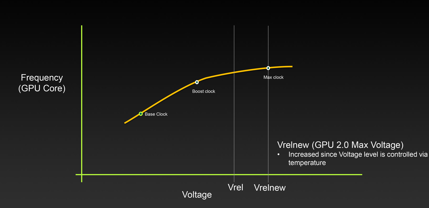
While these voltage points have been present since Kepler, NVIDIA has not, until now, exposed them to end users. However with Pascal this is finally changing, with the introduction of GPU Boost 3.0.
With the latest rendition of NVIDIA’s GPU clockspeed management technology, NVIDIA has made the individual voltage points programmable, and in turn they are exposing this functionality to third party overclocking programs via NVAPI. Consequently it is now possible to adjust the clockspeed of Pascal GPUs at each voltage point, a much greater level of control than before.
The addition of finer-grained controls is designed to improve the flexibility of overclocking on Pascal. Prior to GPU Boost 3.0, the only way to overclock was to adjust the clockspeed for all voltage points by the same amount at the same time – or in NVIDIA’s GPU Boost 3.0 vernacular, a fixed frequency offset. While this certainly works, it limits the highest stable overclock to the lowest point on the voltage/frequency curve. If the GPU can only overclock by 50MHz at the highest voltage point, but 100MHz at a middle point, then the highest stable overclock is only going to be 50MHz.
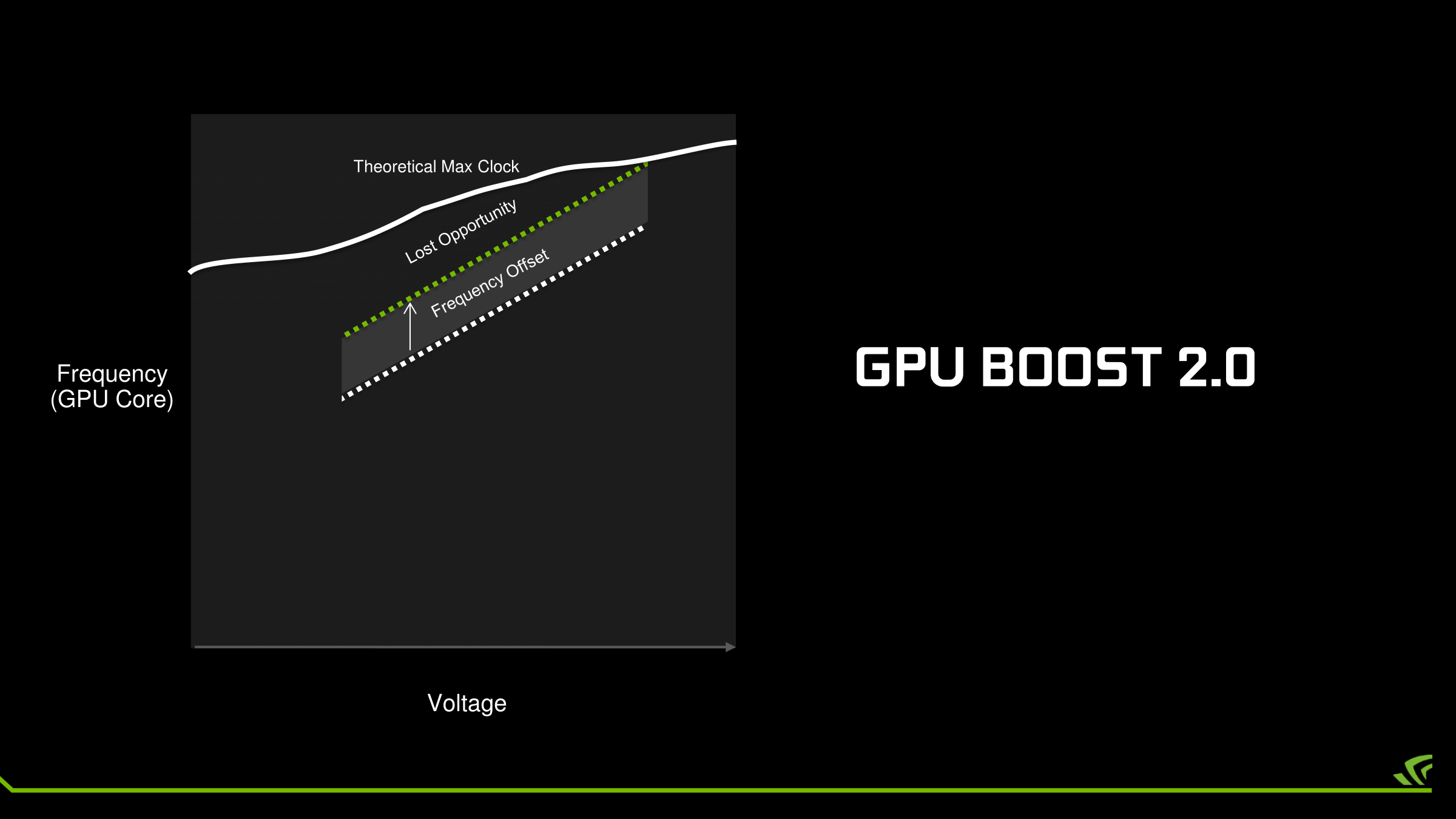
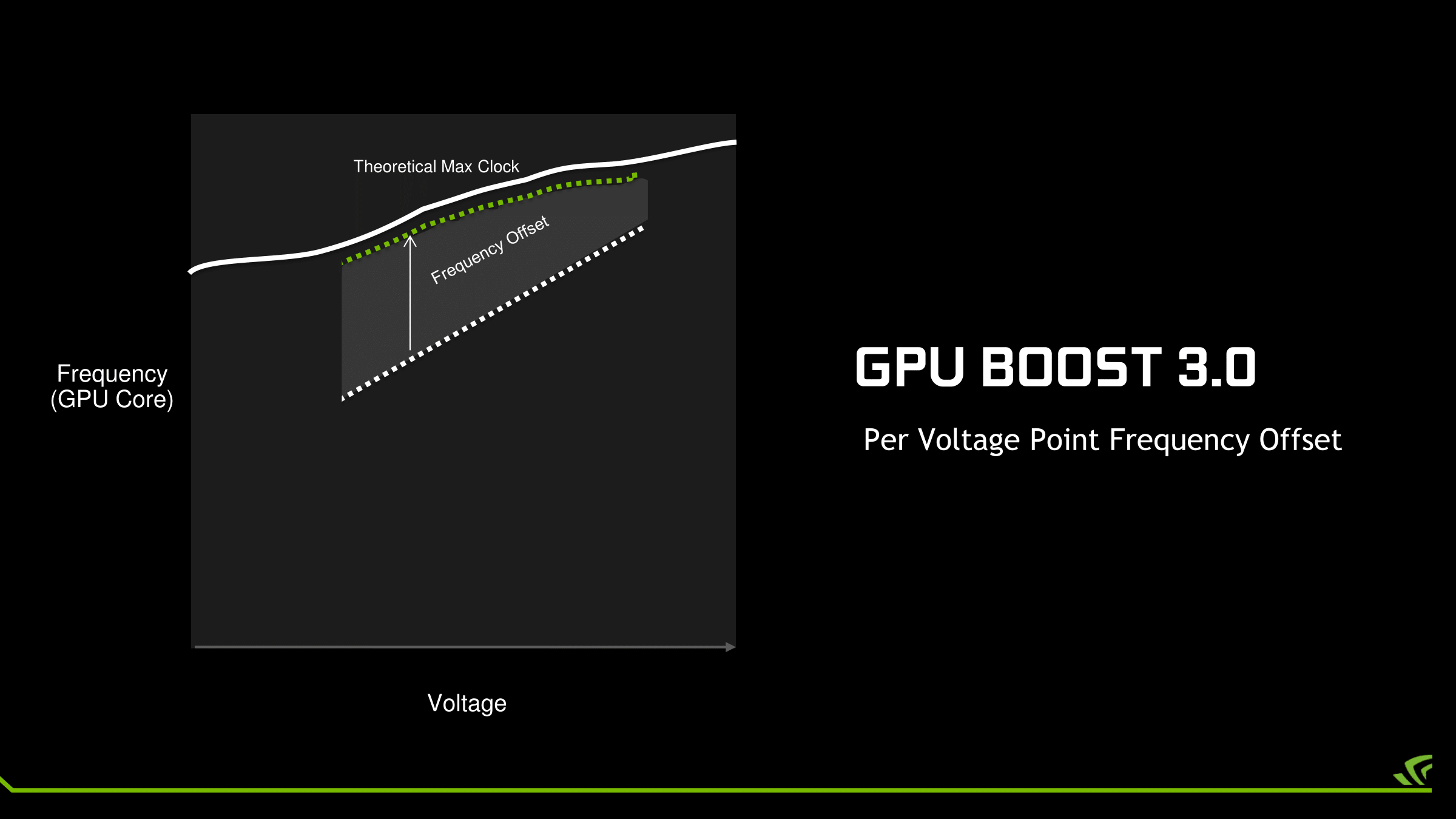
With GPU Boost 3.0 on the other hand, each point on the curve can be adjusted individually. This means the weakest points can be overclocked to a lesser degree while the strongest points can be more significantly overclocked. All other things held equal, this should improve GPU overclocking performance, as GPU tends to shift along multiple points when it’s running. Put another way: GPU Boost 3.0 seeks to wring out the last bits of overclocking headroom along the voltage frequency curve. The only way to go higher still would be to increase the voltage, which NVIDIA hasn’t truly allowed since Fermi.
Meanwhile, the flip side of having finer-grained controls is that it’s now more work to dial in the perfect overclock. Rather than testing one overclock you now have to test nearly two-dozen voltage points to fully exploit GPU Boost 3.0’s abilities, which is time consuming at the best of times. As a result NVIDIA has also exposed a setting in NVAPI to lock the GPU at a specific voltage point. The significance of this is that it now allows overclocking utilities to go through the voltage points and discretely test each one.
The first software to implement this concept is EVGA’s Precision XOC. The latest iteration of EVGA’s overclocking software is able to go through the voltage points and run an OC ScannerX test on each one to find its stability. When a point fails, Precision XOC will then back off the frequency at that point and move on. The end result is that after a series of trials and failures, you should have the virtually-perfect overclock.
Unfortunately while this is sound in concept, in practice NVIDIA and EVGA still aren’t quite there yet. Overclocking failures can cause multiple types of failures; graphic corruption (easy to catch and recover), driver crashes (moderately difficult to recover from), and system hardlocks (very difficult to recover from). In practice, Precision XOC isn’t yet at the point where it can quickly and efficiently handle the last two cases; so driver crashes and system hardlocks still require human intervention, and Precision XOC doesn’t do a great job of resuming from where it left off.
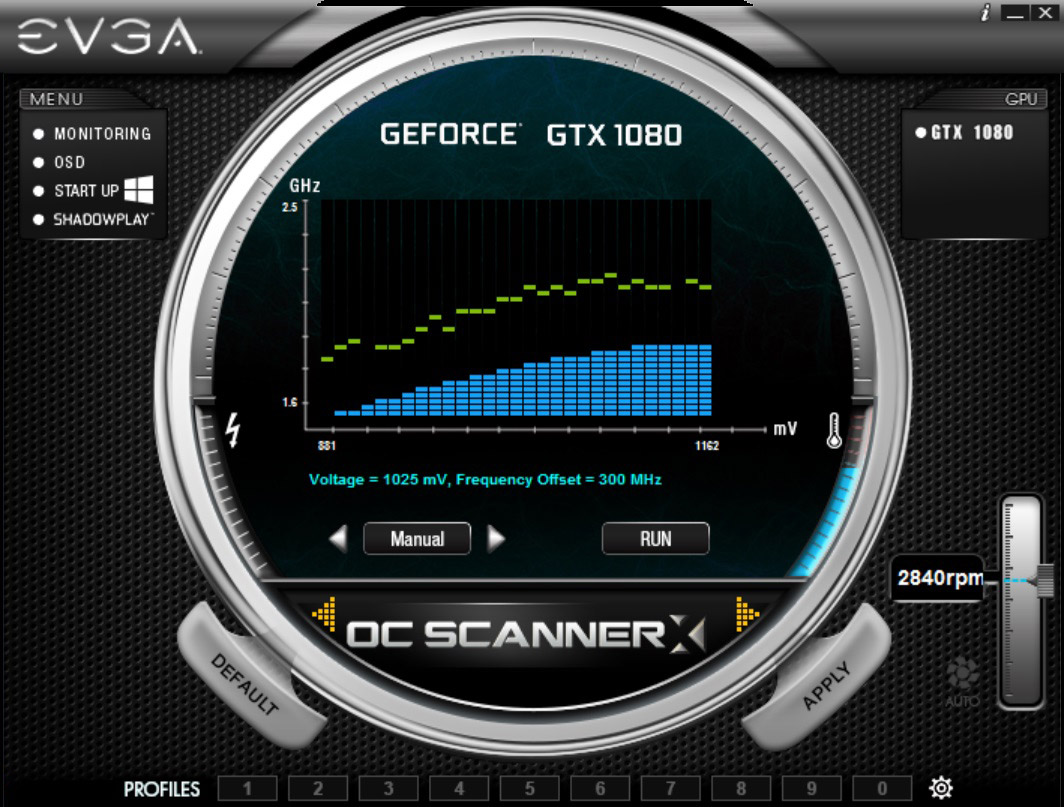
Hopefully one day NVIDIA and EVGA will get there, but for now the only practical way to fully exploit GPU Boost 3.0 is the tedious way. This means either using traditional offset overclocking, or a mode NVIDIA calls linear overclocking, in which the slope of the voltage/frequency curve is adjusted rather than offset (think m in y=mx+b rather than b). In this case two points are picked, and all of the voltage points are overclocked to match the resulting linear curve.
Observations on Clocking with Pascal
While we’re on the subject of clockspeed management on Pascal, I want to discuss my observations with how clockspeeds work on NVIDIA’s newest GPU. When it comes to clockspeed management NVIDIA hasn’t just changed how overclocking works, but relative to Kepler/Maxwell, there are some other, subtle changes.
To start, Pascal clockspeeds are much more temperature-dependent than on Maxwell 2 or Kepler. Kepler would drop a single bin at a specific temperature, and Maxwell 2 would sustain the same clockspeed throughout. However Pascal will drop its clockspeeds as the GPU warms up, regardless of whether it still has formal thermal and TDP headroom to spare. This happens by backing off both on the clockspeed at each individual voltage point, and backing off to lower voltage points altogether.
To quantify this effect, I ran LuxMark 3.1 continuously for several minutes, until the GPU temperature leveled out. As a compute test, LuxMark does not cause the GTX 1080 to hit its 83C temperature limit nor its 180W TDP limit, so it’s a good example of the temperature compensation effect.
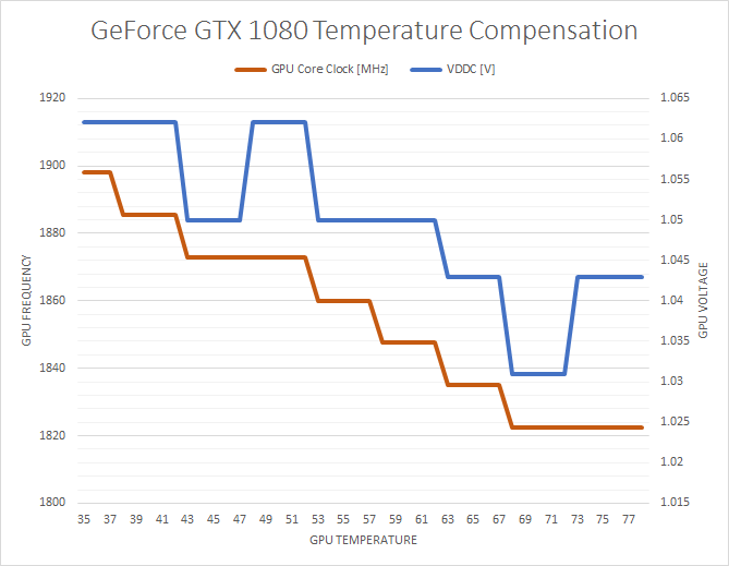
What we find is that from the start of the run until the end, the GPU clockspeed drops from the maximum boost bin of 1898MHz to a sustained 1822MHz, a drop of 4%, or 6 clockspeed bins. These shifts happen relatively consistently up to 68C, after which they stop.
For what it’s worth, the GTX 1080 gets up to 68C relatively quickly, so GPU performance stabilizes rather soon. But this does mean that GTX 1080’s performance is more temperature dependent than GTX 980’s. Throwing a GTX 1080 under water could very well net you a few percent performance increase by avoiding the compensation effect, along with any performance gained from avoiding the card’s 83C temperature throttle.
In any case, I believe this to be compensation for the effects of higher temperatures on the GPU, backing off on voltages/clockspeeds due to potential issues. What those issues are I’m not sure; it could be that 16nm FinFET doesn’t like high voltages at higher temperatures (NVIDIA takes several steps to minimize GPU degradation), or something else entirely.
Otherwise, outside of the temperature compensation effect, clockspeeds on GTX 1080 appear to mostly be a function of temperature or running out of boost bins (VREL limited). The card rarely appears to be TDP limited, especially at steady-state. This indicates that NVIDIA could probably increase the fan speed of the cooler a bit to get a bit more performance, but at the cost of generating a bit more noise.
Finally, how overvolting is being represented is a bit different from before. Previously NVIDIA (and EVGA Precision) would show the exact additional voltage (i.e. the voltage of the unlocked voltage points) when overvolting. However now overvolting is expressed on a percentage scale from 0% to 100%, which obfuscates what the higher voltage points actually are. However this hasn’t changed the underlying behavior of overvolting; one or more voltage points are calibrated by NVIDIA, but they are locked due to the potential for GPU degradation. Overvolting then unlocks these points, allowing the GPU to boost higher so long as there is thermal and power headroom to allow it.


200 Comments
View All Comments
Ryan Smith - Wednesday, July 20, 2016 - link
Thanks.Eden-K121D - Wednesday, July 20, 2016 - link
Finally the GTX 1080 reviewguidryp - Wednesday, July 20, 2016 - link
This echoes what I have been saying about this generation. It is really all about clock speed increases. IPC is essentially the same.This is where AMD lost out. Possibly in part the issue was going with GloFo instead of TSMC like NVidia.
Maybe AMD will move Vega to TSMC...
nathanddrews - Wednesday, July 20, 2016 - link
Curious... how did AMD lose out? Have you seen Vega benchmarks?TheinsanegamerN - Wednesday, July 20, 2016 - link
its all about clock speed for Nvidia, but not for AMD. AMD focused more on ICP, according to them.tarqsharq - Wednesday, July 20, 2016 - link
It feels a lot like the P4 vs Athlon XP days almost.stereopticon - Wednesday, July 20, 2016 - link
My favorite era of being a nerd!!! Poppin' opterons into s939 and pumpin the OC the athlon FX levels for a fraction of the price all while stompin' on pentium. It was a good (although expensive) time to a be a nerd... Besides paying 100 dollars for 1gb of DDR500. 6800gs budget friendly cards, and ATi x1800/1900 super beasts.. how i miss the dayseddman - Thursday, July 21, 2016 - link
Not really. Pascal has pretty much the same IPC as Maxwell and its performance increases accordingly with the clockspeed.Pentium 4, on the other hand, had a terrible IPC compared to Athlon and even Pentium 3 and even jacking its clockspeed to the sky didn't help it.
guidryp - Wednesday, July 20, 2016 - link
No one really improved IPC of their units.AMD was instead forced increase the unit count and chip size for 480 is bigger than the 1060 chip, and is using a larger bus. Both increase the chip cost.
AMD loses because they are selling a more expensive chip for less money. That squeezes their unit profit on both ends.
retrospooty - Wednesday, July 20, 2016 - link
"This echoes what I have been saying about this generation. It is really all about clock speed increases. IPC is essentially the same."- This is a good thing. Stuck on 28nm for 4 years, moving to 16nm is exactly what Nvidias architecture needed.