The NVIDIA GeForce GTX 1080 & GTX 1070 Founders Editions Review: Kicking Off the FinFET Generation
by Ryan Smith on July 20, 2016 8:45 AM ESTGP104: The Heart of GTX 1080
At the heart of the GTX 1080 is the first of the consumer-focused Pascal GPUs, GP104. Though no two GPU generations are ever quite alike, GP104 follows a number of design cues established with the past couple 104 GPUs. Overall 104 GPUs have struck a balance between size and performance, allowing NVIDIA to get a suitably high yielding GPU out at the start of a generation, and to be followed up with larger GPUs later on as yields improve. With the exception of the GTX 780, 104 GPUs been the backbone of NVIDIA’s GTX 70 and 80 parts, and that is once again the case for the Pascal generation.
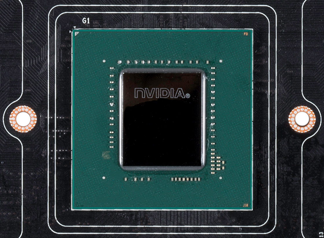
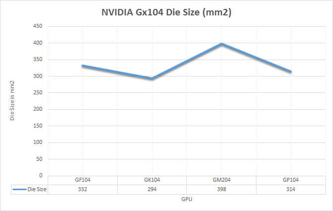
In terms of die size, GP104 comes in at 314mm2. This is right in NVIDIA’s traditional sweet spot for these designs, slotting in between the 294mm2 GK104 and the 332mm2 GF104. In terms of total transistors we’re looking at 7.2B transistors, up from 3.5B on GK104 and the 5.2B of the more unusual GM204. The significant increase in density comes from the use of TSMC’s 16nm FinFET process, which compared to 28nm combines a full node shrink, something that has been harder and harder to come by as the years have progressed.
Though the density improvement offered by TSMC’s 16nm process is of great importance to GP104’s overall performance, for once density takes a back seat to the properties of the process itself. I am of course speaking about the FinFET transistors, which are the headlining feature of TSMC’s process.
We’ve covered FinFET technology in depth before, so I won’t completely rehash it here. But in brief, FinFETs are an important development for chip fabrication as processes have gone below 28nm. As traditional, planar transistors have shrunk in feature size – and ultimately, the number of atoms they’re comprised of – electrical leakage has increased. With fewer atoms in a transistor, there are equally fewer atoms to control the flow of electrons.
FinFET in turn is a solution to this problem, essentially allowing fabs to turn back the clock on electrical leakage. By building transistors as three-dimensional objects with height as opposed to two-dimensional objects, giving FinFET transistors their characteristic fins in the process, FinFET technology greatly reduces the amount of energy a transistor leaks. In practice what this means is that FinFET technology not only reduces the total amount of energy wasted from leakage, but it also allows transistors to be operated at a much lower voltage, something we’ll see in depth with our analysis of GTX 1080.
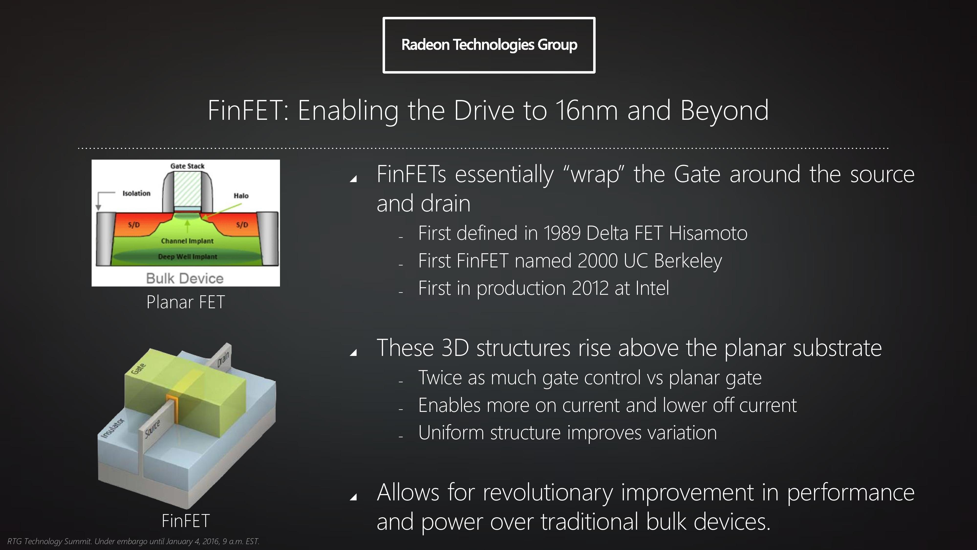
FinFETs, or rather the lack thereof, are a big part of why we never saw GPUs built on TSMC’s 20nm process. It was TSMC’s initial belief that they could contain leakage well enough using traditional High-K Metal Gate (HKMG) technology on 20nm, a bet they ultimately lost. At 20nm, planar transistors were just too leaky to use for many applications, which is why ultimately we only saw SoCs on 20nm (and even then they were suboptimal). FinFETs, as it turns out, are absolutely necessary to get good performance out of transistors built on processes below 28nm.
And while it took TSMC some time to get there, now that they have the capability NVIDIA can reap the benefits. Not only can NVIDIA finally build a relatively massive chip like a GPU on a sub-28nm process, but thanks to the various beneficial properties of FinFETs, it allows them to take their designs in a different direction than what they could do on 28nm.


200 Comments
View All Comments
Robalov - Tuesday, July 26, 2016 - link
Feels like it took 2 years longer than normal for this review :Dextide - Wednesday, July 27, 2016 - link
The venn diagram is wrong -- for GP104 it says 1:64 speed for FP16 -- it is actually 1:1 for FP16 (ie same speed as FP32) (NOTE: GP100 has 2:1 FP16 -- meaning FP16 is twice as fast as FP32)extide - Wednesday, July 27, 2016 - link
EDIT: I might be incorrect about this actually as I have seen information claiming both .. weird.mxthunder - Friday, July 29, 2016 - link
its really driving me nuts that a 780 was used instead of a 780ti.yhselp - Monday, August 8, 2016 - link
Have I understood correctly that Pascal offers a 20% increase in memory bandwidth from delta color compression over Maxwell? As in a total average of 45% over Kepler just from color compression?flexy - Sunday, September 4, 2016 - link
Sorry, late comment. I just read about GPU Boost 3.0 and this is AWESOME. What they did, is expose what previously was only doable with bios modding - eg assigning the CLK bins different voltages. The problem with overclocking Kepler/Maxwell was NOT so much that you got stuck with the "lowest" overclock as the article says, but that simply adding a FIXED amount of clocks across the entire range of clocks, as you would do with Afterburner etc. where you simply add, say +120 to the core. What happened here is that you may be "stable" at the max overclock (CLK bin), but since you added more CLKs to EVERY clock bin, the assigned voltages (in the BIOS) for each bin might not be sufficient. Say you have CLK bin 63 which is set to 1304Mhz in a stock bios. Now you use Afterburner and add 150 Mhz, now all of a sudden this bin amounts to 1454Mhz BUT STILL at the same voltage as before, which is too low for 1454Mhz. You had to manually edit the table in the BIOS to shift clocks around, especially since not all Maxwell cards allowed adding voltage via software.Ether.86 - Tuesday, November 1, 2016 - link
Astonishing review. That's the way Anandtech should be not like the mobile section which sucks...Warsun - Tuesday, January 17, 2017 - link
Yeah looking at the bottom here.The GTX 1070 is on the same level as a single 480 4GB card.So that graph is wrong.http://www.hwcompare.com/30889/geforce-gtx-1070-vs...
Remember this is from GPU-Z based on hardware specs.No amount of configurations in the Drivers changes this.They either screwed up i am calling shenanigans.
marceloamaral - Thursday, April 13, 2017 - link
Nice Ryan Smith! But, my question is, is it truly possible to share the GPU with different workloads in the P100? I've read in the NVIDIA manual that "The GPU has a time sliced scheduler to schedule work from work queues belonging to different CUDA contexts. Work launched to the compute engine from work queues belonging to different CUDA contexts cannot execute concurrently."marceloamaral - Thursday, April 13, 2017 - link
Nice Ryan Smith! But, my question is, is it truly possible to share the GPU with different workloads in the P100? I've read in the NVIDIA manual that "The GPU has a time sliced scheduler to schedule work from work queues belonging to different CUDA contexts. Work launched to the compute engine from work queues belonging to different CUDA contexts cannot execute concurrently."