The NVIDIA GeForce GTX 1080 & GTX 1070 Founders Editions Review: Kicking Off the FinFET Generation
by Ryan Smith on July 20, 2016 8:45 AM ESTPascal’s Architecture: What Follows Maxwell
With the launch of a new generation of GPUs we’ll start things off where we always do: the architecture.
Discrete GPUs occupy an interesting space when it comes to the relationship between architecture and manufacturing processes. Whereas CPUs have architecture and manufacturing process decoupled – leading to Intel’s aptly named (former) tick-tock design methodology – GPUs have aligned architectures with manufacturing processes, with a new architecture premiering alongside a new process. Or rather, GPU traditionally did. Maxwell threw a necessary spanner into all of this, and in its own way Pascal follows this break from tradition.
As the follow-up to their Kepler architecture, with Maxwell NVIDIA introduced a significantly altered architecture, one that broke a lot of assumptions Kepler earlier made and in the process vaulted NVIDIA far forward on energy efficiency. What made Maxwell especially important from a development perspective is that it came not on a new manufacturing process, but rather on the same 28nm process used for Kepler two years earlier, and this is something NVIDIA had never done before. With the 20nm planar process proving unsuitable for GPUs and only barely suitable for SoCs – the leakage from planar transistors this small was just too high – NVIDIA had to go forward with 28nm for another two years. It would come down to their architecture team to make the best of the situation and come up with a way to bring a generational increase in performance without the traditional process node shrink.
Now in 2016 we finally have new manufacturing nodes with the 14nm/16nm FinFET processes, giving GPU manufacturers a long-awaited (and much needed) opportunity to bring down power consumption and reduce chip size through improved manufacturing technology. The fact that it has taken an extra two years to get here, and what NVIDIA did in the interim with Maxwell, has opened up a lot of questions about what would follow for NVIDIA. The GPU development process is not so binary or straightforward that NVIDIA designed Maxwell solely because they were going to be stuck on the 28nm process – NVIDIA would have done Maxwell either way – but it certainly was good timing to have such a major architectural update fall when it did.
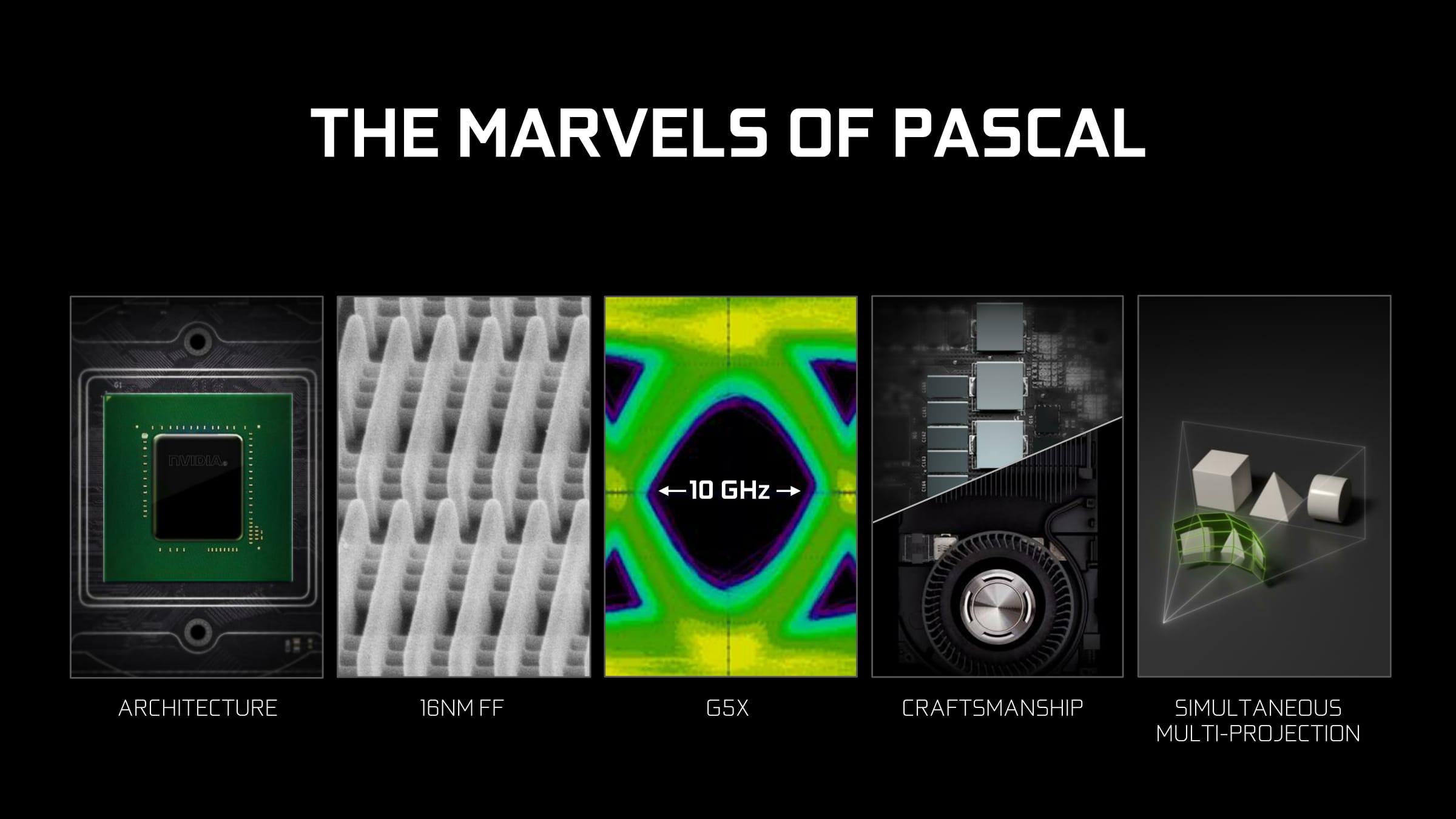
So how does NVIDIA follow-up on Maxwell then? The answer comes in Pascal, NVIDIA’s first architecture for the FinFET generation. Designed to be built on TSMC’s 16nm process, Pascal is the latest and the greatest, and like every architecture before it is intended to further push the envelope on GPU performance, and ultimately push the envelope on the true bottleneck for GPU performance, energy efficiency.
HPC vs. Consumer: Divergence
Pascal is an architecture that I’m not sure has any real parallel on a historical basis. And a big part of that is because to different groups within NVIDIA, Pascal means different things and brings different things, despite the shared architecture. On the one side is the consumer market, which is looking for a faster still successor to what Maxwell delivered in 2014 and 2015. Meanwhile on the high performance compute side, Pascal is the long-awaited update to the Kepler architecture (Maxwell never had an HPC part), combining the lessons of Maxwell with the specific needs of the HPC market.
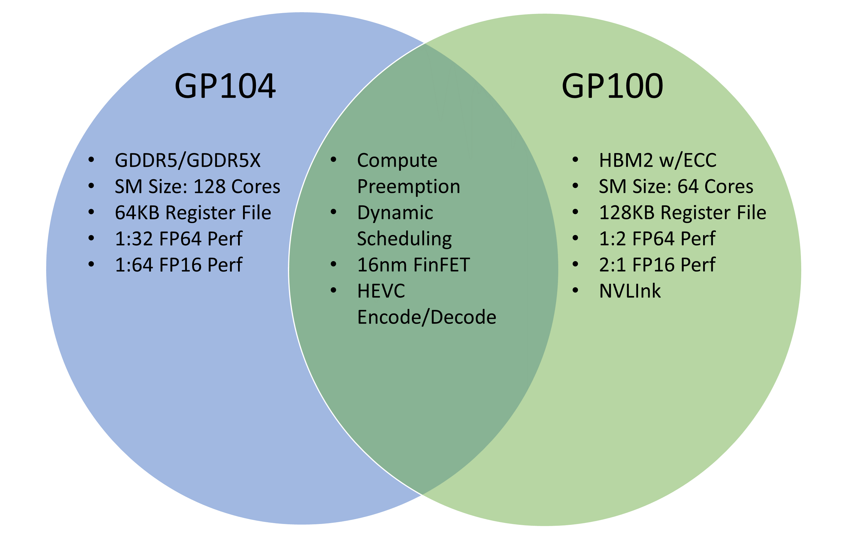
The result is that there’s an interesting divergence going on between the HPC side and its GP100 GPU, and the consumer side and the GP104 GPU underlying GTX 1080. Even as far back as Fermi there was a distinct line separating HPC-class GPUs (GF100) from consumer/general compute GPUs (GF104), but with Pascal this divergence is wider than ever before. Ultimately the HPC market and GP100 is beyond the scope of this article and I’ll pick it up in detail another time, but because NVIDIA announced GP100 before GP104, it does require a bit of addressing to help sort out what’s going on and what NVIDA’s design goals were with GP104.
Pascal as an overarching architecture contains a number of new features, however not all of those features are present in all SKUs. If you were to draw a Venn diagram of Pascal, what you would find is that the largest collection of features are found in GP100, whereas GP104, like the previous Maxwell architecture before it, is stripped down for speed and efficiency. As a result while GP100 has some notable feature/design elements for HPC – things such faster FP64 & FP16 performance, ECC, and significantly greater amounts of shared memory and register file capacity per CUDA core – these elements aren’t present in GP104 (and presumably, future Pascal consumer-focused GPUs).
Ultimately what we’re seeing in this divergence is a greater level of customization between NVIDIA’s HPC and consumer markets. The HPC side of NVIDIA is finally growing up, and it’s growing fast. The long term plan at NVIDIA has been to push GPU technology beyond consumer and professional graphics, and while it has taken years longer than NVIDIA originally wanted, thanks in big part to success in the deep learning market, NVIDIA is finally achieving their goals.
This means that although GP100 is a fully graphics capable GPU, it doesn’t necessarily have to be put into video cards to make sense for NVIDIA to manufacture, and as a result NVIDIA can make it even more compute focused than prior-generation parts like GK110 and GF110. And that in turn means that although this divergence is driven by the needs of the HPC market – what features need to be added to make a GPU more suitable for HPC use cases – from the perspective of the consumer market there is a tendency to perceive that consumer parts are falling behind. Especially with how GP100 and GP104’s SMs are differently partitioned.
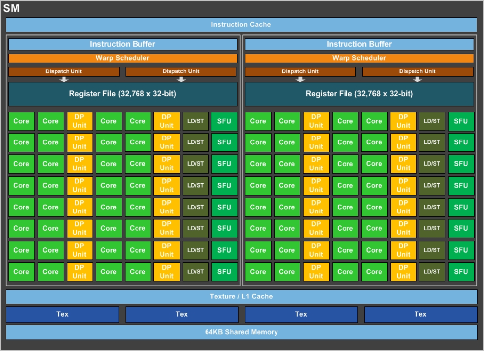
This is a subject I’ll revisit in much greater detail in the future when we focus on GP100. But for now, especially for the dozen of you who’ve emailed over the past month asking about why the two are so different, the short answer is that the market needs for HPC are different from graphics, and the difference in how GP100 and GP104 are partitioned reflect this. GP100 and GP104 are both unequivocally Pascal, but GP100 gets smaller SM partitions in order to increase the number of registers and the amount of shared memory available per CUDA core. Shared memory and register contention on graphics workloads isn’t nearly as great as with HPC tasks – pixel shader threads are relatively short and independent from each other – which means that while the increased ratios benefit HPC workloads, for graphics the gains would be minimal. And the costs to power and die space would, in turn, far outweigh any benefits.


200 Comments
View All Comments
grrrgrrr - Wednesday, July 20, 2016 - link
Solid review! Some nice architecture introductions.euskalzabe - Wednesday, July 20, 2016 - link
The HDR discussion of this review was super interesting, but as always, there's one key piece of information missing: WHEN are we going to see HDR monitors that take advantage of these new GPU abilities?I myself am stuck at 1080p IPS because more resolution doesn't entice me, and there's nothing better than IPS. I'm waiting for HDR to buy my next monitor, but being 5 years old my Dell ST2220T is getting long in the teeth...
ajlueke - Wednesday, July 20, 2016 - link
Thanks for the review Ryan,I think the results are quite interesting, and the games chosen really help show the advantages and limitations of the different architectures. When you compare the GTX 1080 to its price predecessor, the 980 Ti, you are getting an almost universal ~25%-30% increase in performance.
Against rival AMDs R9 Fury X, there is more of a mixed bag. As the resolutions increase the bandwidth provided by the HBM memory on the Fury X really narrows the gap, sometimes trimming the margin to less that 10%,s specifically in games optimized more for DX12 "Hitman, "AotS". But it other games, specifically "Rise of the Tomb Raider" which boasts extremely high res textures, the 4Gb memory size on the Fury X starts to limit its performance in a big way. On average, there is again a ~25%-30% performance increase with much higher game to game variability.
This data lets a little bit of air out of the argument I hear a lot that AMD makes more "future proof" cards. While many Nvidia 900 series users may have to upgrade as more and more games switch to DX12 based programming. AMD Fury users will be in the same boat as those same games come with higher and higher res textures, due to the smaller amount of memory on board.
While Pascal still doesn't show the jump in DX12 versus DX11 that AMD's GPUs enjoy, it does at least show an increase or at least remain at parity.
So what you have is a card that wins in every single game tested, at every resolution over the price predecessors from both companies, all while consuming less power. That is a win pretty much any way you slice it. But there are elements of Nvidia’s strategy and the card I personally find disappointing.
I understand Nvidia wants to keep features specific to the higher margin professional cards, but avoiding HBM2 altogether in the consumer space seems to be a missed opportunity. I am a huge fan of the mini ITX gaming machines. And the Fury Nano, at the $450 price point is a great card. With an NVMe motherboard and NAS storage the need for drive bays in the case is eliminated, the Fury Nano at only 6” leads to some great forward thinking, and tiny designs. I was hoping to see an explosion of cases that cut out the need for supporting 10-11” cards and tons of drive bays if both Nvidia and AMD put out GPUs in the Nano space, but it seems not to be. HBM2 seems destined to remain on professional cards, as Nvidia won’t take the risk of adding it to a consumer Titan or GTX 1080 Ti card and potentially again cannibalize the higher margin professional card market. Now case makers don’t really have the same incentive to build smaller cases if the Fury Nano will still be the only card at that size. It’s just unfortunate that it had to happen because NVidia decided HBM2 was something they could slap on a pro card and sell for thousands extra.
But also what is also disappointing about Pascal stems from the GTX 1080 vs GTX 1070 data Ryan has shown. The GTX 1070 drops off far more than one would expect based off CUDA core numbers as the resolution increases. The GDDR5 memory versus the GDDR5X is probably at fault here, leading me to believe that Pascal can gain even further if the memory bandwidth is increased more, again with HBM2. So not only does the card limit you to the current mini-ITX monstrosities (I’m looking at you bulldog) by avoiding HBM2, it also very likely is costing us performance.
Now for the rank speculation. The data does present some interesting scenarios for the future. With the Fury X able to approach the GTX 1080 at high resolutions, most specifically in DX12 optimized games. It seems extremely likely that the Vega GPU will be able to surpass the GTX 1080, especially if the greatest limitation (4 Gb HBM) is removed with the supposed 8Gb of HBM2 and games move more and more the DX12. I imagine when it launches it will be the 4K card to get, as the Fury X already acquits itself very well there. For me personally, I will have to wait for the Vega Nano to realize my Mini-ITX dreams, unless of course, AMD doesn’t make another Nano edition card and the dream is dead. A possibility I dare not think about.
eddman - Wednesday, July 20, 2016 - link
The gap getting narrower at higher resolutions probably has more to do with chips' designs rather than bandwidth. After all, Fury is the big GCN chip optimized for high resolutions. Even though GP104 does well, it's still the middle Pascal chip.P.S. Please separate the paragraphs. It's a pain, reading your comment.
Eidigean - Wednesday, July 20, 2016 - link
The GTX 1070 is really just a way for Nvidia to sell GP104's that didn't pass all of their tests. Don't expect them to put expensive memory on a card where they're only looking to make their money back. Keeping the card cost down, hoping it sells, is more important to them.If there's a defect anywhere within one of the GPC's, the entire GPC is disabled and the chip is sold at a discount instead of being thrown out. I would not buy a 1070 which is really just a crippled 1080.
I'll be buying a 1080 for my 2560x1600 desktop, and an EVGA 1060 for my Mini-ITX build; which has a limited power supply.
mikael.skytter - Wednesday, July 20, 2016 - link
Thanks Ryan! Much appreciated.chrisp_6@yahoo.com - Wednesday, July 20, 2016 - link
Very good review. One minor comment to the article writers - do a final check on grammer - granted we are technical folks, but it was noticeable especially on the final words page.madwolfa - Wednesday, July 20, 2016 - link
It's "grammar", though. :)Eden-K121D - Thursday, July 21, 2016 - link
Oh the ironychrisp_6@yahoo.com - Thursday, July 21, 2016 - link
oh snap, that is some funny stuff right there