The ASUS Maximus VIII Extreme Review: The Other $500 Option
by Ian Cutress on April 7, 2016 9:00 AM EST- Posted in
- Motherboards
- Gaming
- Asus
- ROG
- Skylake
- Z170
- Thunderbolt 3
Visual Inspection
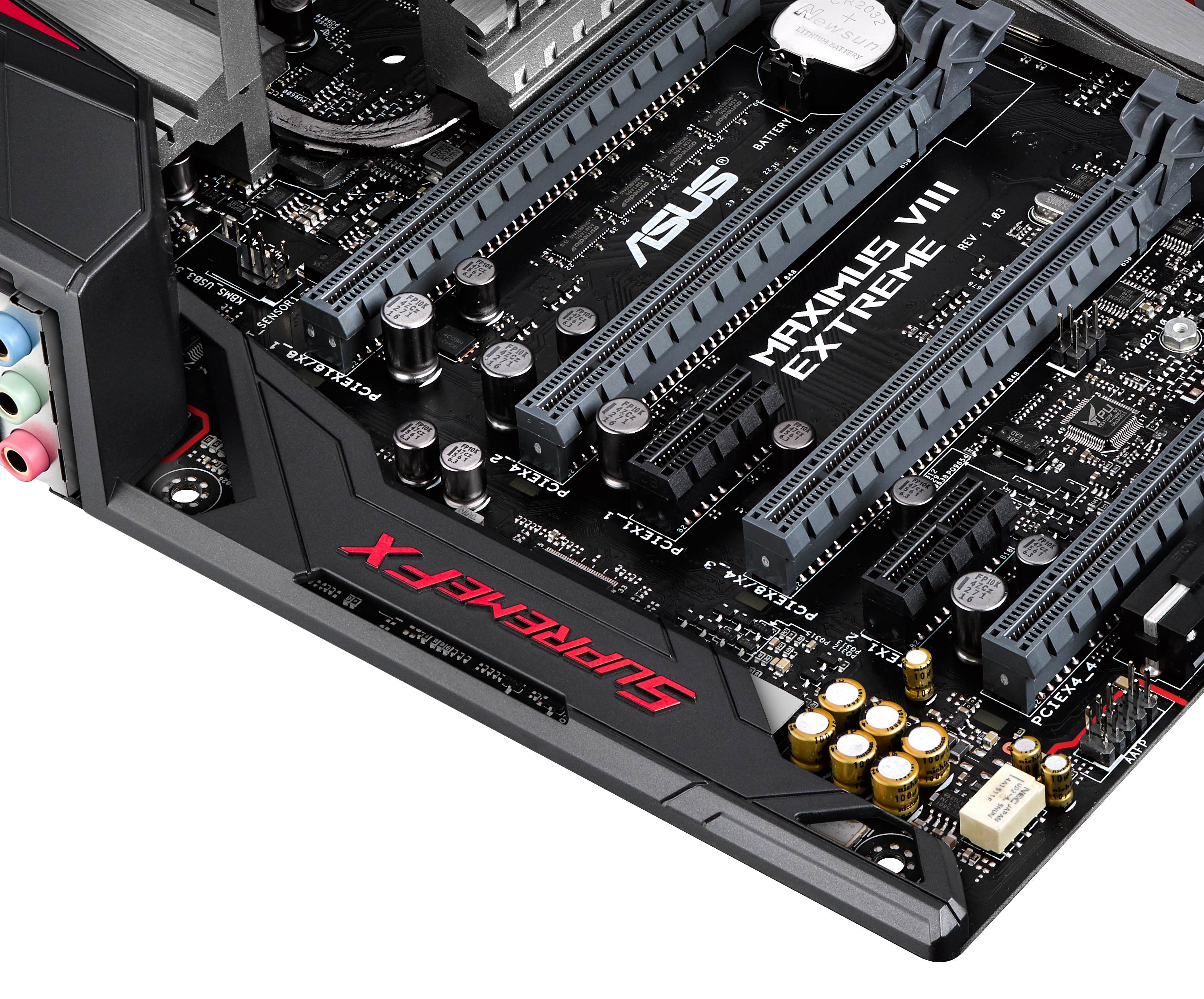
As mentioned on the first page in the overview, ASUS is moving the Extreme line into something a little more reserved and subtle, but still with a feeling of bulk and utility. We saw this with the Rampage IV Black Edition, although the full black look is at the other end of the scale. The M8E comes in more refined, using a consistent black and grey coloring across the heatsinks, DRAM slots, PCIe slots, SATA ports and USB 3.0 headers to make sure everything looks in place. Grey can be boring however, so the look has red highlights and accents on the heatsinks using the angular motif and design ASUS has liked to use in the past couple of years. While the ‘Maximus VIII’ and ‘Extreme’ name is recessed into the grey heatsink, the ‘SupremeFX’ name is raised in red, with the ROG logo on the chipset heatsink recessed but hiding an RGB LED underneath. Using the software, users can make this logo pulse a number of colors for looks, or turn it off to create a stealth-like system.
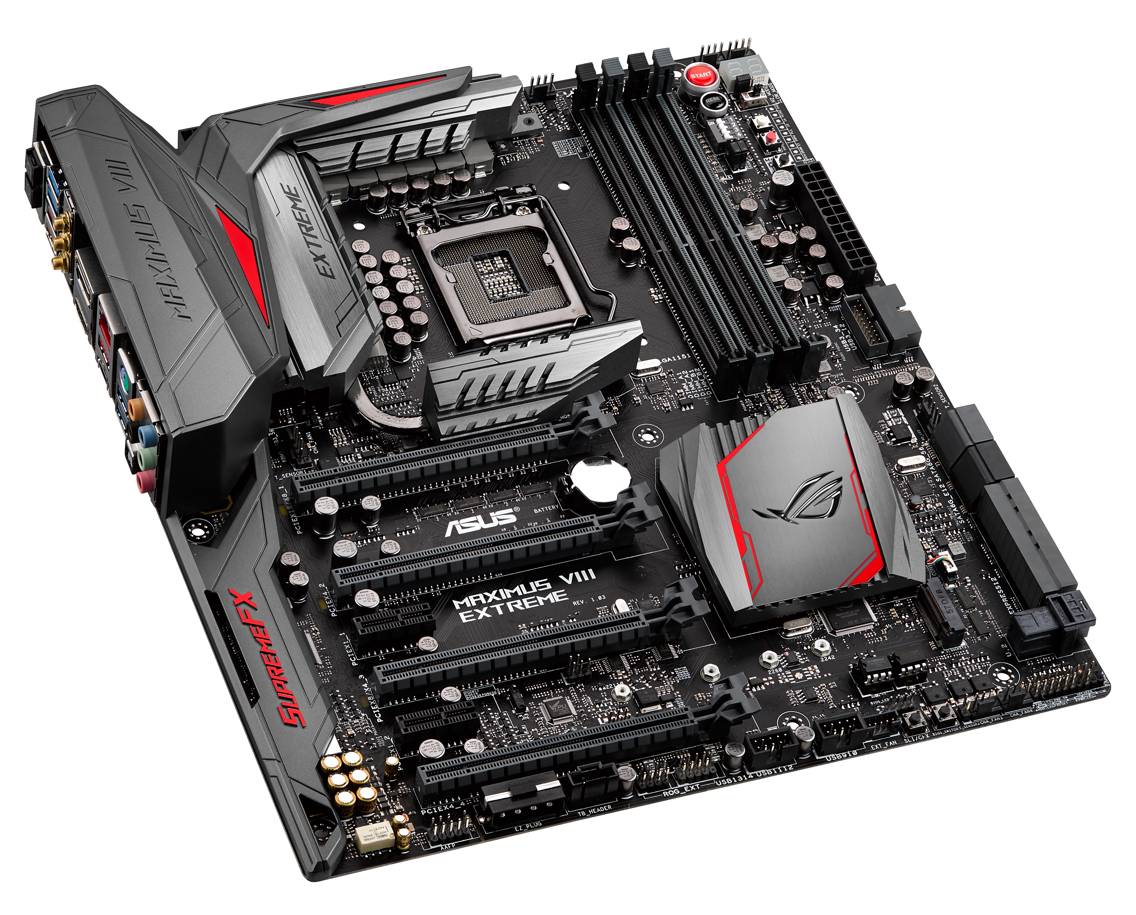
The power delivery heatsinks around the socket cover three sides and encompass the rear I/O cover as well. This cover extends down to the audio segment of the motherboard, purely because the rear I/O and audio can be two of the biggest culprits for disturbing aesthetics. It should be noted that the heatsink below the socket is in the area normally reserved for a PLX8747 chip which would enable 3-way and 4-way SLI by multiplexing the PCIe lanes. The fact that all the PCIe 3.0 slots are full-length might suggest that a PLX chip is present, as this is a common connection. However, there is no PLX chip here. The first three PCIe slots use sixteen lanes from the CPU and operate in x16, x8/-/x8 or x8/x4/x4 modes while the last slot is an x4 implementation from the chipset. For SLI, due to NVIDIA’s restrictions, eight PCIe lanes are needed at a minimum. This means we are limited to 2-way SLI here.
Of the six fan headers onboard, the socket area has quick access to four of them – two 4-pin CPU headers and a 4-pin chassis header in the top right and a 4-pin chassis header just above the first PCIe slot. The final two headers are at the bottom of the motherboard, both 4-pin.
The power delivery, by virtue of being a motherboard that ASUS expects extreme users to overclock using liquid nitrogen on, is hyper-engineered as a result.
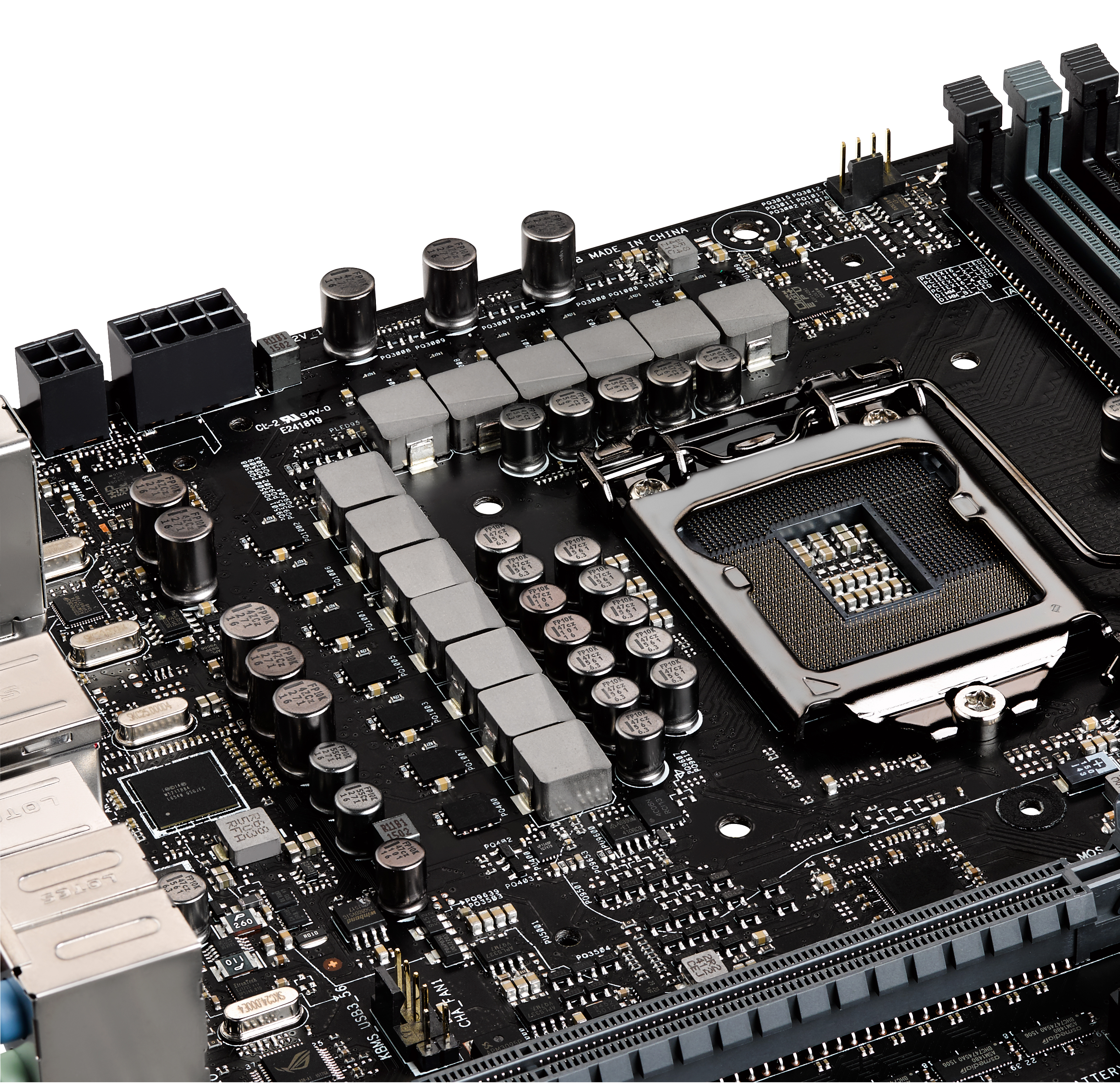
The thirteen phases here are most likely in a 12+1 configuration, with the 12 being multiplexed as 2x6 or 3x4. Where ASUS’ main competitor uses International Rectifier chokes and PWMs, ASUS combines MicroFine alloy chokes (provides a predictable voltage response) with Infineon OptiMOS MOSFETs for a higher current drain and dual PWM controllers for finer CPU and CPU graphics voltage adjustments. There’s also 10K black capacitors there, rated for 10000 days compared to 2000 on regular motherboards, but at this price most motherboards will have 5k/8k/10k/12k implementations depending on the motherboard manufacturer.
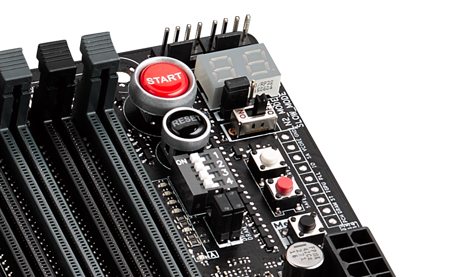
On the top right of the motherboard are the DRAM slots and a number of the enthusiast options. The start/reset buttons are standard on most motherboards above $150, as is the two-digit debug display. Below the reset button is a set of DIP switches for PCIe slots, allowing enthusiasts to disable certain PCIe slots if needed (usually to remove potential erratic behavior in sub-zero mode, or if GPUs can’t be removed but an overclocking run on a single GPU is needed). Below this is a pair of jumpers, used for enabling/disabling specific memory channels.
Next to this is an LN2 mode jumper, which when enabled will give more BIOS options related to liquid nitrogen overclocking as well as provide certain setting safeguards. Below this is a slow mode switch, forcing the processor into a low-frequency state (typically 800 MHz) which guarantees booting into an operating system. Typically extreme overclockers will use this in two ways – either to debug a bad overclock, or to implement an extreme overclock for a short time/short benchmark before taking a score before going back to slow mode to ensure the system is stable enough to take a screenshot of their benchmark score for overclocking leagues.
The nine silver dots below this are the onboard voltage read points. Overclockers use these with their multimeters to read the voltage of certain parts of the system (core, graphics, DRAM, chipset, system agent) which might not be read correctly by software. As some overclockers will be adjusting frequency and voltage on the fly, this is a way of detecting that the voltage required is set properly. Next to these are a set of three buttons, linked to ASUS’ ReTry, Safe_Boot and Mem_OK features for recovering an unstable system.
A note on the DRAM slots – they are single side latched, meaning that users should be aware if their memory is firmly inserted on both sides (the upside of this is making it easier to remove memory when a full-length large GPU is being used which blocks the bottom latches if present).
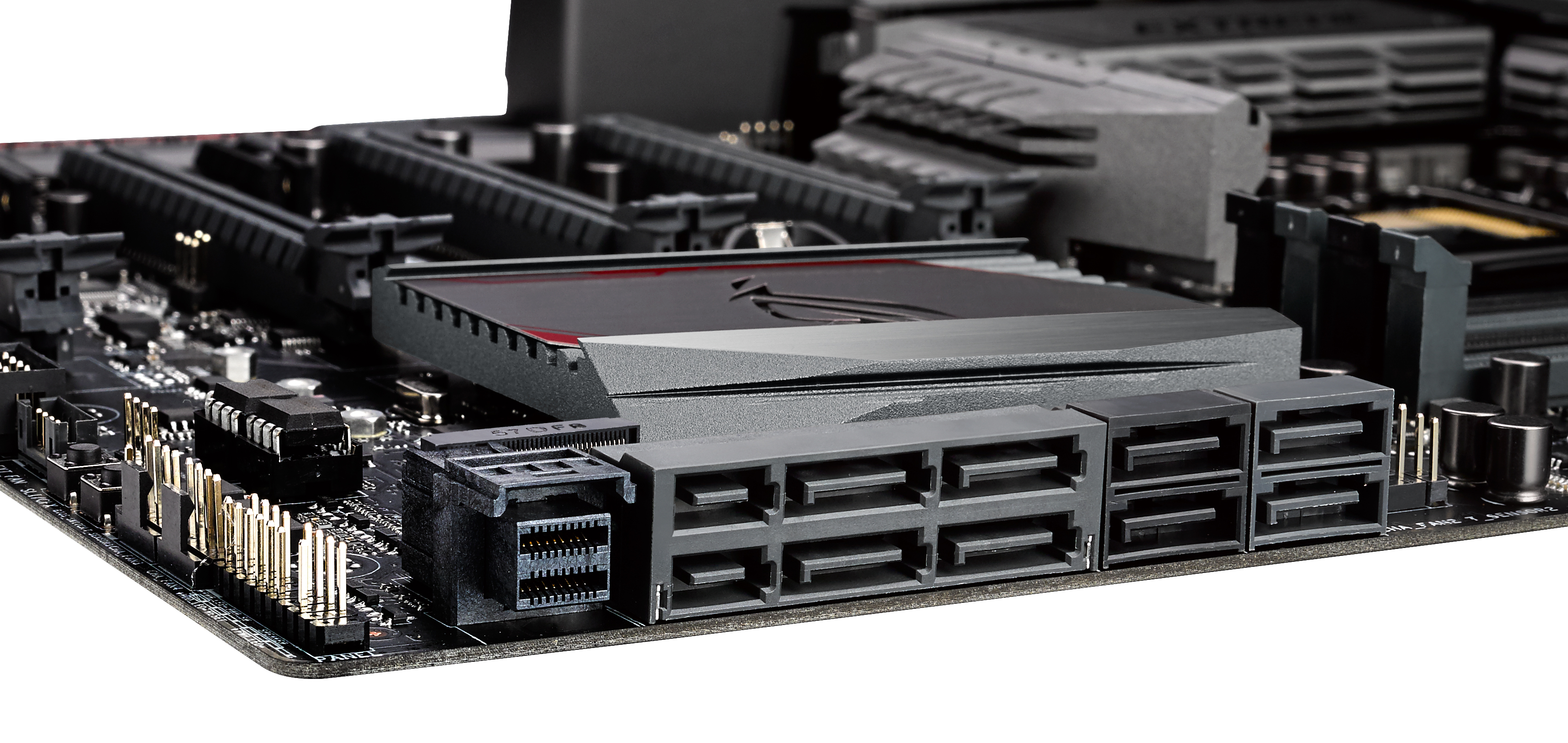
Moving down the right-hand side of the board there are two USB 3.0 headers, one at right angles, for built-in case ports. Below this are the SATA ports, combined with two SATA Express ports, then a U.2 port. The SATA ports in black come from an ASMedia controller, whereas the rest are provided by the chipset. If we ignore SATA Express (because everyone should at this point), the important thing here is U.2. As a new (new-ish) standard for storage offering PCIe 3.0 x4 bandwidth, I have a strong feeling that motherboards will slowly migrate this way depending on chipset bandwidth. As shown in the image above, it takes the place of two SATA ports for one U.2 drive, and comes in at the same height. We are in an age where motherboards easily come with six or more SATA ports, most of which remain unused, while a U.2 drive (2.5-inch or 3.5-inch) could run into the terabytes for storage under a single cable. U.2 is ultimately competing with M.2, but we are waiting for the main SSD companies to release their U.2 devices which can offer more storage and better cooling characteristics in exchange for volume and PC location. Intel already released the SSD 750 (which is one more released drive over SATA Express which has zero), we are just waiting on others. U.2, on the whole, is more of an enterprise play. The cables are more expensive than SATA (~$1 vs $0.02 in bulk), which increases the cost, but I find that a minor argument if we can get high-speed multi-TB storage. It is worth noting at this time that Intel does not have a PCIe SSD controller smaller than 22mm, so if 3D XPoint ever comes to consumers, either Intel needs a new PCIe controller for M.2 or it will be U.2 only until then.
On the audio side, ASUS hides most of it under the SupremeFX shield, but underneath holds an enhanced Realtek ALC1150 implementation using an ESS ES9023P DAC via a bypass. The solution also includes enhanced filter caps, a headphone amplifier and a sense amp to allow for 32-600 ohm headphones. There is also PCB separation of the digital/analog sections of the motherboard and gold-plated audio connectors.
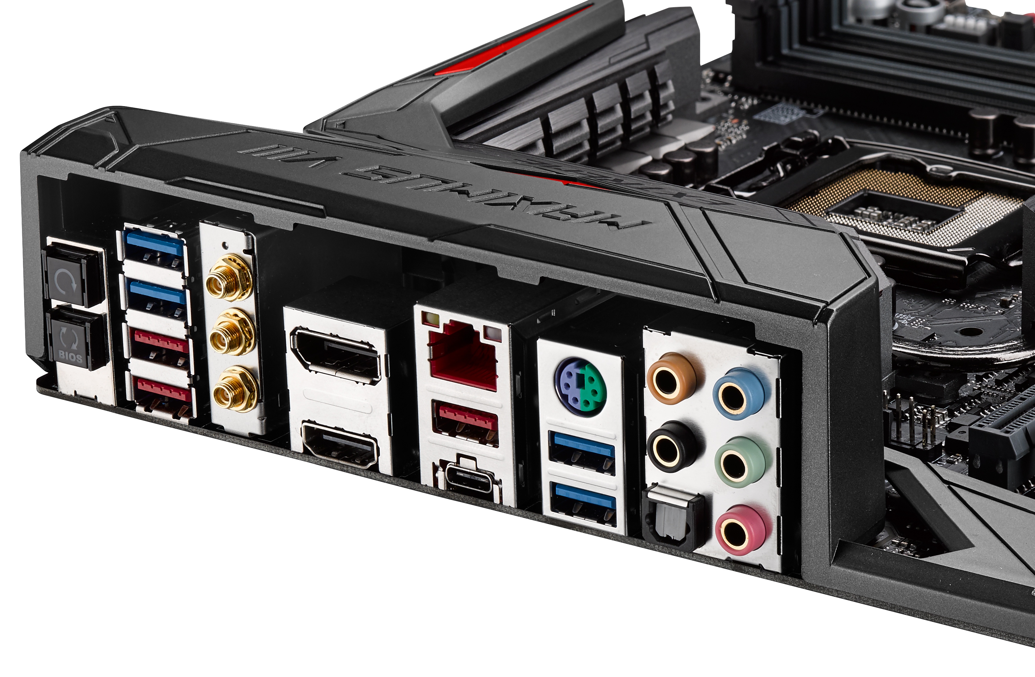
On the rear panel we an interesting display – zero USB 2.0 ports. Instead we have one of the few motherboards with more than two USB 3.1 ports, here showing two Type-A ports in red on the left from an ASMedia ASM1142 controller and then a Type-A and Type-C from Intel’s Alpine Ridge controller. That Type-C port is also qualified for Thunderbolt 3 support up to 40 Gbps using an active cable. The blue ports are USB 3.0 ports from the chipset, and we also get an Intel I219-V network port and a PS/2 combination port. On the far left are two buttons with the top one resetting the BIOS and the bottom one allowing for ASUS’ USB BIOS Flashback which can flash a BIOS without a CPU, DRAM or GPU present. Elsewhere on the rear panel is the 3T3R Wi-Fi Go module, a Displayport/HDMI port for onboard graphics, and the audio jacks.


Test Setup
| Test Setup | |
| Processor | Intel Core i7-6700K (ES, Retail Stepping), 91W, $350 4 Cores, 8 Threads, 4.0 GHz (4.2 GHz Turbo) |
| Motherboards | ASUS Maximus VIII Impact |
| Cooling | Cooler Master Nepton 140XL |
| Power Supply | OCZ 1250W Gold ZX Series Corsair AX1200i Platinum PSU |
| Memory | Corsair DDR4-2133 C15 2x8 GB 1.2V or G.Skill Ripjaws 4 DDR4-2133 C15 2x8 GB 1.2V |
| Memory Settings | JEDEC @ 2133 |
| Video Cards | ASUS GTX 980 Strix 4GB MSI GTX 770 Lightning 2GB (1150/1202 Boost) ASUS R7 240 2GB |
| Hard Drive | Crucial MX200 1TB |
| Optical Drive | LG GH22NS50 |
| Case | Open Test Bed |
| Operating System | Windows 7 64-bit SP1 |
Readers of our motherboard review section will have noted the trend in modern motherboards to implement a form of MultiCore Enhancement / Acceleration / Turbo (read our report here) on their motherboards. This does several things, including better benchmark results at stock settings (not entirely needed if overclocking is an end-user goal) at the expense of heat and temperature. It also gives in essence an automatic overclock which may be against what the user wants. Our testing methodology is ‘out-of-the-box’, with the latest public BIOS installed and XMP enabled, and thus subject to the whims of this feature. It is ultimately up to the motherboard manufacturer to take this risk – and manufacturers taking risks in the setup is something they do on every product (think C-state settings, USB priority, DPC Latency / monitoring priority, overriding memory sub-timings at JEDEC). Processor speed change is part of that risk, and ultimately if no overclocking is planned, some motherboards will affect how fast that shiny new processor goes and can be an important factor in the system build.
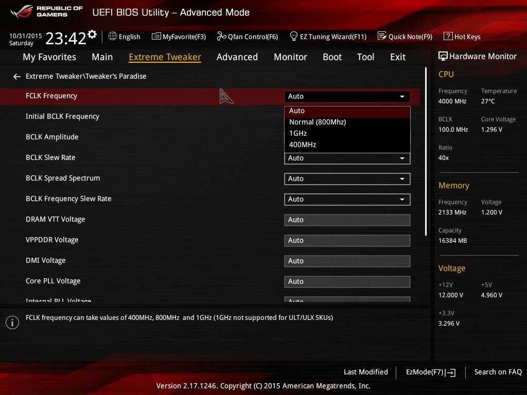
For reference, the ASUS Maximus VIII Extreme, on our testing BIOS 1101, MCT was enabled by default. Also, the FCLK 10x ratio was present in the BIOS tested at the time of testing.
Many thanks to...
We must thank the following companies for kindly providing hardware for our test bed:
Thank you to AMD for providing us with the R9 290X 4GB GPUs.
Thank you to ASUS for providing us with GTX 980 Strix GPUs.
Thank you to ASRock and ASUS for providing us with some IO testing kit.
Thank you to Cooler Master for providing us with Nepton 140XL CLCs.
Thank you to Corsair for providing us with an AX1200i PSU.
Thank you to Crucial for providing us with MX200 SSDs.
Thank you to G.Skill and Corsair for providing us with memory.
Thank you to MSI for providing us with the GTX 770 Lightning GPUs.
Thank you to OCZ for providing us with PSUs.
Thank you to Rosewill for providing us with PSUs and RK-9100 keyboards.


70 Comments
View All Comments
willis936 - Thursday, April 7, 2016 - link
Well if you dump a grand on an extreme processor and not half a grand on a board you could get 8 cores that OC up to the same as the K series parts. Double the threaded performance but same single threaded performance.bill.rookard - Thursday, April 7, 2016 - link
I would have to agree, unless you are a hardcore overclocker. For those interested in hugely powerful graphics setups, this doesn't really cut it (dual GPU SLI only). For those who want huge storage arrays, this doesn't cut it either (half dozen SATA ports). Those interested in liquid nitrogen overclocks and need those last few mhz would find a use for it though...Chaitanya - Friday, April 8, 2016 - link
Normally I would have agreed, spending more than 250$ on Z/P series chipsets is useless and its better to go to X platform. But in this case there seems to be a good value in terms of bundle. That 10G Nic is worth the extra. There are no X99 boards below $500 mark that come with 10G nics.romrunning - Thursday, April 7, 2016 - link
"The cost of an i7-6700K plus a $500 motherboard comes in at $750 MSRP, "These prices seem really off. As of today, Amazon has the list price of the i7-6700k as $419.99. Simple math gets you to $919.99 with a $500 mobo, not $750.
Ian Cutress - Thursday, April 7, 2016 - link
Box price for 6700K is $350 (we've been covering the ups and downs of the price of the Skylake parts, see the link on the first page, where from time to time it is hitting MSRP), making it more $850, so I'm $100 out :) Updated. It's sill a big jump between the two, for sure.romrunning - Thursday, April 7, 2016 - link
So now I had to check Intel's "Recommended Customer Price" for the i7-5820k. Intel's site says box price is $396. So that + a $250 m/b would make the combo around $650, not $550. That would lower the different to more around $200. Still not insignificant, as that is the price of a decent m/b, but less than the previous cited difference.romrunning - Thursday, April 7, 2016 - link
Also, thanks for adding in the pricing info. It helps to give a measure of worth to the end-user to know the premium they are paying & what essentially you are buying over a more standard board.ImSpartacus - Friday, April 8, 2016 - link
I think he meant a 6600K.BrokenCrayons - Thursday, April 7, 2016 - link
Yes, $500 isn't exactly a princely sum, but I don't see value in spending that much on a single component of a computer. That's a week's play money for outings, shopping, and casual dining. Using it instead to buy a motherboard of all things only demonstrates to others in your social circles that you don't quite have your priorities sorted out. So thanks for the effort ASUS, but no thanks.Questor - Thursday, April 7, 2016 - link
Yes, blowing that much money on frivolous casual dining, outings and shopping is obviously a demonstration of financial brilliance! Priorities are as different among people as personal beliefs or political views. I won't pay the premium for this motherboard either, especially without dual M.2 slots to RAID NVMe SSDs. The OC Panel is unwanted bling to me as well, but I can see other people finding the M8E to be their "thing."