The Intel Xeon E5 v4 Review: Testing Broadwell-EP With Demanding Server Workloads
by Johan De Gelas on March 31, 2016 12:30 PM EST- Posted in
- CPUs
- Intel
- Xeon
- Enterprise
- Enterprise CPUs
- Broadwell
Broadwell-EP: A 10,000 Foot View
What are the building blocks of a 22-core Xeon? The short answer: 24 cores, 2.5 MB L3-cache per core, 2 rings connected by 2 bridges (s-boxes) and several PCIe/QPI/home "agents".
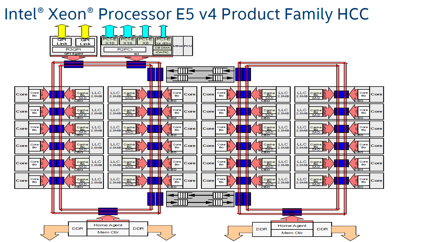
The fact that only 22 of those 24 cores are activated in the top Xeon E5 SKU is purely a product differentiation decision. The 18 core Xeon E5 v3 used exactly the same die as the Xeon E7, and this has not changed in the new "Broadwell" generation.
The largest die (+/- 454 mm²), highest core (HCC) count SKUs still work with a two ring configuration connected by two bridges. The rings move data in opposite directions (clockwise/counter-clockwise) in order to reduce latency by allowing data to take the shortest path to the destination. The blue points indicate where data can jump onto the ring buses. Physical addresses are evenly distributed over the different cache slices (each 2.5 MB) to make sure that L3-cache accesses are also distributed, as a "hotspot" on one L3-cache slice would lower performance significantly. The L3-cache latency is rather variable: if the core is lucky enough to find the data in its own cache slice, only one extra cycle is needed (on top of the normal L1-L2-L3 latency). Getting a cacheline of another slice can cost up to 12 cycles, with an average cost of 6 cycles..
Meanwhile rings and other entities of the uncore work on a separate voltage plane and frequency. Power can be dynamically allocated to these entities, although the uncore parts are limited to 3 GHz.
Just like Haswell-EP, the Broadwell-EP Xeon E5 has three different die configurations. The second configuration supports 12 to 15 cores and is a smaller version (306mm²) of the third die configuration that we described above. These dies still have two memory controllers.
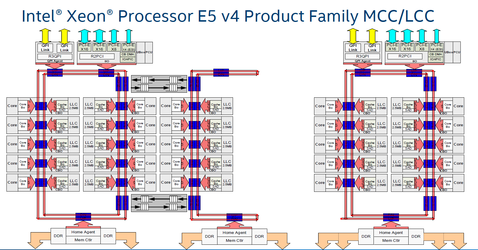
Otherwise the smallest 10 core die uses only one dual ring, two columns of cores, and only one memory controller. However, the memory controller drives 4 channels instead of 2, so there is a very small bandwidth penalty (5-10%) compared to the larger dies (HCC+MCC) with two memory controllers. The smaller die has a smaller L3-cache of course (25 MB max.). As the L3-cache gets smaller, latency is also a bit lower.
Cache Coherency
As the core count goes up, it gets increasingly complex to keep cache coherency. Intel uses the MESIF (Modified, Exclusive, shared, Invalid and Forward) protocol for cache coherency. The Home Agents inside the memory controller and the caching agents inside the L3-cache slice implement the cache coherency. To maintain consistency, a snoop mechanism is necessary. There are now no less than 4 different snoop methods.
The first, Early Snoop, was available starting with Sandy Bridge-EP models. With early snoop, caching agents broadcast snoop requests in the event of an L3-cache miss. Early snoop mode offers low latency, but it generates massive broadcasting traffic. As a result, it is not a good match for high core count dies running bandwidth intensive applications.
The second mode, Home Snoop, was introduced with Ivy Bridge. Cache line requests are no longer broadcasted but forwarded to the home agent in the home node. This adds a bit of latency, but significantly reduces the amount of cache coherency traffic.
Haswell-EP added a third mode, Cluster on Die (CoD). Each home agent has 14 KB directory cache. This directory cache keeps track of the contested cache lines to lower cache-to-cache transfer latencies. In the event of a request, it is checked first, and the directory cache returns a hit, snoops are only sent to indicated (by the directory cache) agents.
On Broadwell-EP, the dice are indeed split along the rings: all cores on one ring are one NUMA node, all other cores on the other ring make the second NUMA node. On Haswell-EP, the split was weirder, with one core of the second ring being a member of the first cluster. On top of that, CoD splits the processor in two NUMA nodes, more or less one node per ring.
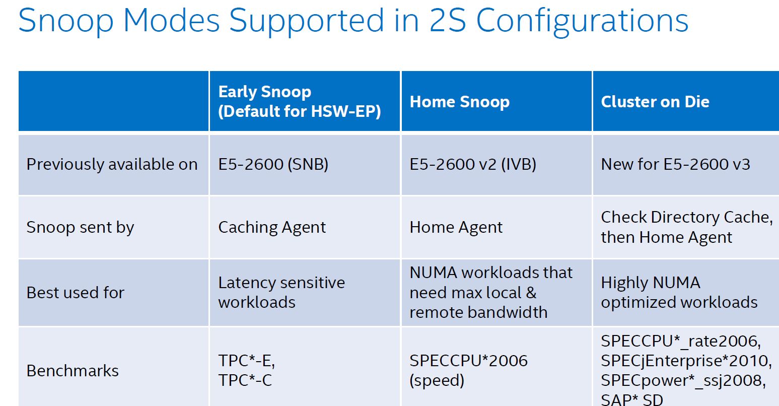
The fourth mode, introduced with Broadwell EP, is the "home snoop" method, but improved with the use of the directory cache and yet another refinement called opportunistic snoop broadcast. This mode already starts snoops to the remote socket early and does the read of the memory directory in parallel instead of waiting for the latter to be done. This is the default snoop method on Broadwell EP.
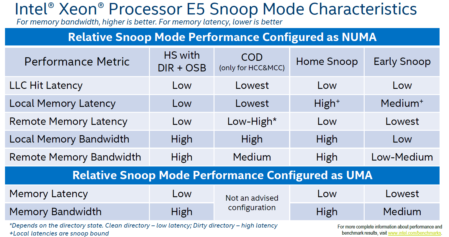
This opportunistic snooping lowers the latency to remote memory.
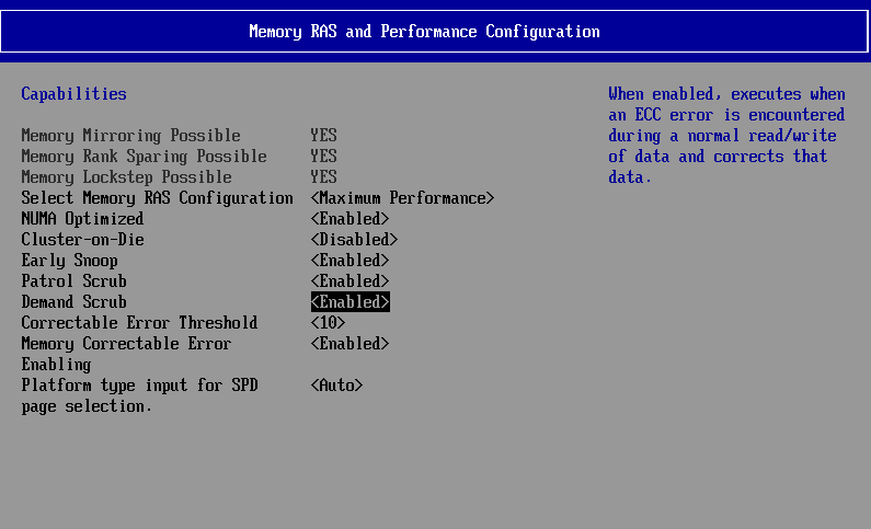
These snoop modes can be set in the BIOS as you can see above.


112 Comments
View All Comments
PowerOfFacts - Thursday, June 23, 2016 - link
And now Oracle marketing speaks. Their HammerDB results are bogus. Oracle continues to site socket results when the majority of the world has moved on to per core results. They cite the results from a 32 core HammerDB then compare it to a 1 chip (1/2 of 1 socket) POWER8 because Phil has a hard-on for how "HE" believes IBM has packaged the processor and similarly chooses an Intel configuration to ensure "THEY" get the result they want. Phil & Oracle (appear) to always speak with forked tongue.patrickjp93 - Sunday, April 3, 2016 - link
"Best" only at specific scale-up workloads. There's a reason Sparc is not particularly popular for clusters and supercomputing (and it's NOT software compatibility). It sucks at a lot of workloads when compared to x86. As for the SAP benchmarks, that's to be expected since x86 doesn't yet support transactional memories. That changes with Skylake Purley though.Brutalizer - Wednesday, April 6, 2016 - link
In these 25ish benchmarks, the SPARC M7 is 2-3x faster on all kinds of workloads, not just some specific scale up workloads. The reason SPARC M7 is not popular for clusters (supercomputers are clusters) is not because of low raw compute performance, it is because of cost and wattage. The M7 is much more expensive than x86, and draws much more power. I guess somewhere 250 watt or so? M7 are in big enterprise servers, some have water cooling, etc. Whereas clusters have many cheap nodes, with no water cooling.Clusters can have x86 because the highest wattage x86 cpu, uses 140 watt or so. Not more. So it would be feasible to use 140 watt cpus in clusters. But not 250 watt cpus, they draw too much power.
For instance, the IBM Blue Gene supercomputer that hold spot nr 5 in top500 for a couple of years, used 850 MHz powerpc cpus, when everyone else used 2.4 GHz x86 or so. The 850 MHz cpu dont use lot of power, so that is the reason it was used in Blue Gene, not because it was faster (it wasnt). A large supercomputer can draw 10 MegaWatt, and that costs very much. Power is a huge issue in super computers. SPARC M7 draws too much power to be useful in a large cluster, and costs too much.
If we talk about raw compute power for SPARC M7, it reaches 1200 SPECint2006, whereas E5-2699v3 reaches 715 SPECint2006. Not really 2-3x faster, but still much faster.
In SPECfp2006, the M7 reaches 832, whereas the E5-2699v3 reach 474.
https://blogs.oracle.com/BestPerf/entry/201510_spe...
So, as you can see yourself, the SPARC M7 is faster on scale-up business workloads (it was designed for that type of workloads) and also faster on raw compute power. And faster in everything in between. Just look at the wide diversity among these 25 ish benchmarks.
Brutalizer - Wednesday, April 6, 2016 - link
BTW, do you really expect a 150 watt x86 cpu, to outperform a 250 watt SPARC M7 cpu? Have you seen benchmarks where they compare 250 watt graphics card vs a 150 watt graphics card? Which GPU do you think is faster? Do you expect a 150 watt GPU to outperform a 250 watt gpu?The SPARC M7 has 50% more cores, twice the cpu cache, twice the GHz, twice the Wattage, twice the RAM bandwidth, twice the nr of transistors (10 billions) - and you are surprised it is 2-3x faster than x86?
BTW, the SPARC M7 has stronger cores than x86. If you look at all these benchmarks, typically one M7 with 32 cores, is faster than two E5-2699v3 with 2x18 = 36 cores. This must mean that one SPARC M7 core, packs more punch than a E5-2699v3 core, because 32 SPARC cores are faster than 36 x86 cores in all benchmarks.
adamod - Friday, June 3, 2016 - link
i know this is an old post but i am confused (this isnt something i have learned much about yet) i am hoping you can help some...if the sparc has 2 to 3x performance and is 250w compared to 140w then wouldnt that make it MORE efficient? and if you need two 2699's to compare to a sparc m7 then wouldnt that be 280w, more than the 250w of the xeons? i realize there are other factors here but this doesnt make sense to me. also yea there are graphics cards that are a lower wattage and perform better...i am an AMD fan but nvidia has had some faster cards with better performance in the past...i have an R9 280X, a mid grade card rated at i believe 225w, kinda crazy when it can get beaten by 17w nvidia cardstqth - Sunday, April 3, 2016 - link
The SPARC and POWER servers are for people with unlimited pocket where compactness and reliability worth the premium it's spent on. If you have to ask how much it costs, you'd probably can't afford it.Xeons are commodity hardware where you could purchase the best bang for your buck.
They are not aiming at the same market. Most software wouldn't even work on both system.
Besides, benchmarks are worthless - unless the performance of the specific software is tested. And that's rare.
PowerOfFacts - Thursday, June 23, 2016 - link
Depends on which Xeon processors you are referring to. The latest Broadwell EP & EX chips can cost over $7K each. Well on par if not exceeding POWER8 chips and definitely more than OpenPOWER chips. Times are changing. Intel has milked their clients for a long time feeding them the marketing line of open, commodity & low cost. They are no longer open buying up ecosystem integrating into the silicone, what exactly does commodity mean anyway and as low cost goes ... as I just said, pretty salty.yuhong - Thursday, March 31, 2016 - link
64GB LR-DIMMs will probably not come out at reasonable prices until 8Gbit DDR4 is more mainstream.iwod - Thursday, March 31, 2016 - link
I thought Samsung announced a 128GB DIMM with some type of 3D / TSV RAM.Casper42 - Thursday, March 31, 2016 - link
Not shipping just yet though.Should be sometime this year though.