Examining Soft Machines' Architecture: An Element of VISC to Improving IPC
by Ian Cutress on February 12, 2016 8:00 AM EST- Posted in
- CPUs
- Arm
- x86
- Architecture
- Soft Machines
- IPC
The Data: Soft Machines' Proof
Ever since the initial announcement of the VISC architecture in 2014 there has been a element of it sounding too good to be true, and Soft Machines' 2016 announcements have come with yet more questions as well. Aside from questions requiring more information about the architecture and ISA, the big money questions relate to performance. We mentioned a couple of pages back that the original 28nm design made its way to silicon at 500 MHz and was shown as a proof of concept. At the 2014 conference, the platform was compared to both ARM and x86 and offered better scores on Denbench compared to both while also using less power. Now that Shasta is on the 16nm node, the big question is how the new design at a 2 GHz frequency compares, and if the increase in frequency has upset some of the IPC gains.
So it’s at this point that we have to show this graph before we can progress any further. This is a graph which has caused a lot of commotion among the analyst community, because it can be a very difficult graph to digest and work out what is going on. I’ll take you through it. But to start, ignore the vertical dashed lines.
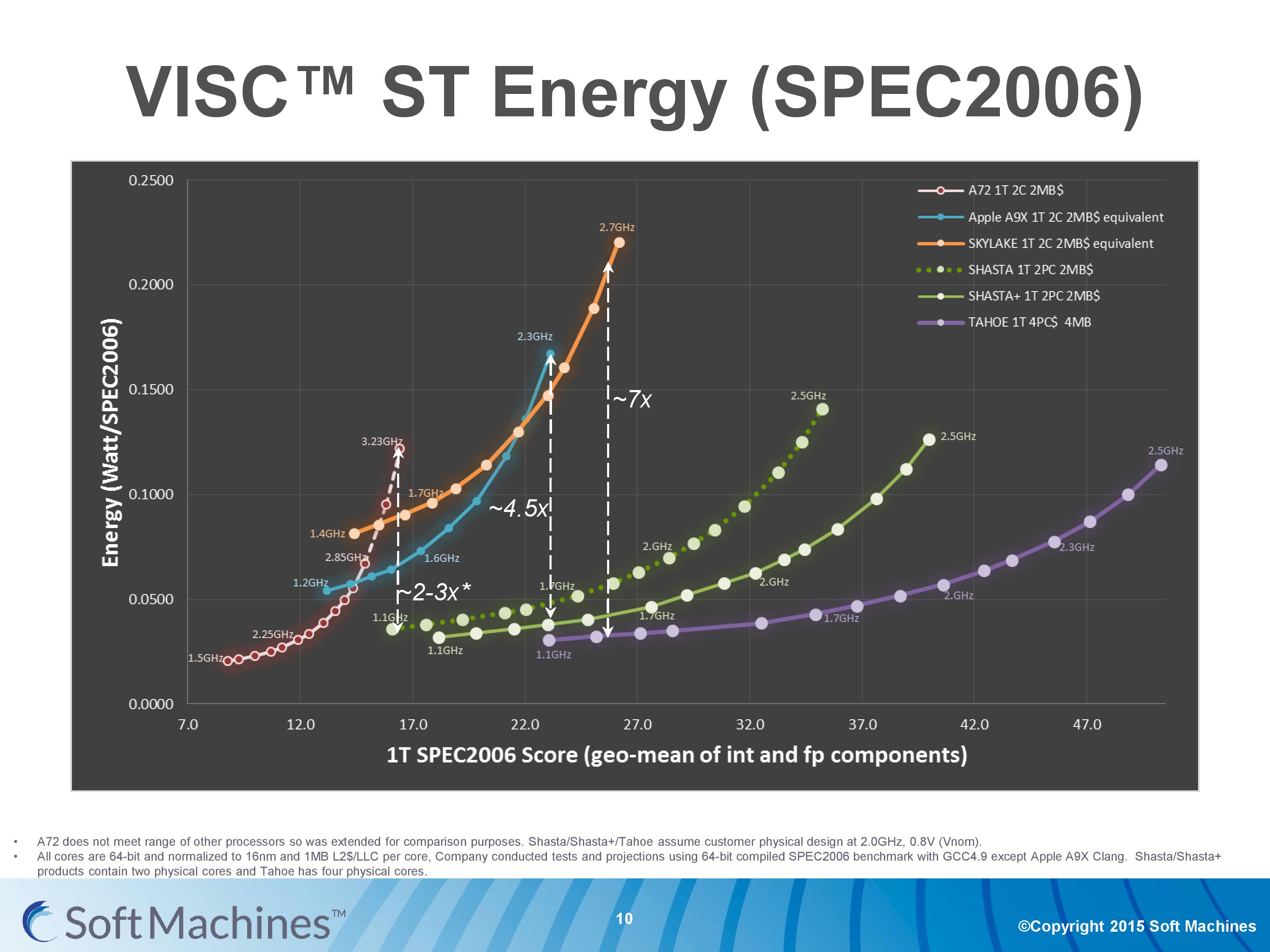
This is a graph from Soft Machines attempting to show the efficiency of several CPUs cores: Cortex-A72, Apple’s Twister (A9X), Skylake, Shasta, Shasta+ (2017), and Tahoe (2018). It is a graph of the average power consumed per unit SPEC2006 score plotted against the SPEC2006 score, and each dot on a line shows the relative score of each CPU at a given frequency.
The reason why this graph has caused a lot of commotion is that it shows a lot of data based on a lot of assumptions displayed in a very odd way. The following points are worth mentioning
| The Scores #1 | This graph shows the geometric mean of SPEC2006int and SPEC2006fp, the integer and floating point parts of the SPEC2006 set of benchmark tools. Because different architectures focus on integer and floating point performance to differing degrees (more units focused on INT or FP), these results are typically given separately, with individual subtest scores. Practically no-one in the industry puts them together as a geometric mean, which has some analysts wondering if there are certain subtests where VISC scores particularly low. |
| The Scores #2 | This graph shows only single threaded results, even though each CPU is listed as having two cores in the data but running a single thread. This puts the Soft Machines cores in the best light, as a single thread has access to all the ports on two cores as well as two re-order buffers and two cores' worth of L2 cache. |
| Conversion #1 | All the results have been converted as if each CPU design has 1MB of last level cache per core. This means that designs such as the A9X and Skylake CPUs have been reduced, and scores have been adjusted by ambiguous ‘industry standard techniques’ according to SMI. A number of analysts say that this is not a fair conversion, as an A9X core or Skylake core with less cache would be arranged differently in silicon to take advantage of more space for other things or lower latencies. |
| Conversion #2 | All the results have been converted to 16nm FinFET+ on TSMC, again by ‘industry standard techniques’. This is a hard one to grasp, because core designs are not simply ‘shrunk’ from one node to another. Similar to the cache situation, each process node can be optimized for metal layers and arrangement for latency and bandwidth optimizations. Each conversion, such as Intel’s 14nm to TSMC 16nm, or TSMC’s 28nm -> 16nm, would have to be thoroughly examined. Extrapolating from 28nm to 16nm would be an exasperating task to be accurate (and this level of extrapolation wouldn’t be acceptable even in a high school classroom as I pointed out). |
| Testing #1 | Not all points on the graph come from direct data. Each line has had several points taken from data and the rest are interpolated given basic power formulas. |
| Testing #2 | The platforms used are not all what they appear to be. So for example, the best Cortex-A72 16nm data point would be the Kirin 950 in the Huawei Mate 8, but instead a dual A72 was used from the Amazon Fire TV which as a 28nm MediaTek MT8173 running at 1.98 GHz. One could argue that A72 is new enough and only recently on 28nm that it isn’t fully optimized for the process yet and this is probably a low end version of that silicon. The Apple A9X numbers are actually taken from a 14nm A9 and the assumption was made that the dynamic power in a cold environment was similar to the A9X. The Skylake numbers were a mid-range Core i5-6200U in a Dell laptop, which could be prone to variable turbo modes or overheating, and that specific SKU is hardly the most power efficient model in Intel’s Skylake lineup. |
| Compilers | In order to ‘normalize’ the data, each of the actual data points taken were as a result of SPEC2006 being compiled on GCC 4.9 (or Clang for Apple). Typically for SPEC we normally consider the peak numbers possible with the best compiler, and as pointed out by some analysts, Intel’s results on their compiler can get scores more than double that of GCC, which can put a negative bent on Intel’s numbers. |
| Simulations | Almost all of SMI’s numbers come from internal RTL simulation of their IP designs. With the 28nm proof-of-concept chip, we were told that the difference between simulation and physical was around 5-10% on performance and power, but some chip designers have pointed out that performance on a simulated processor can be anywhere from 33-50% inaccurate from the peak theoretical performance when you actually put it into silicon. |
| Optimizations | The data shown in this graph for the VISC processors is based on assumptions relating to process optimization. The way the design is to be sold means that licensees can work with the foundries to optimize the metal stack layers or other design characteristics to get better power or higher frequencies. I was told that this was put into the graph at an assumed value around 10%, and the data in the graph includes this. |
Typically any one of these points in most contexts would be grounds to be apprehensive about the results. The fact that there are nine salient points here listed (and I may even have missed one or two) means that the data should be thrown out entirely.
Clarification on the Data from Soft Machines
Because we were one of the last media outlets to speak with Soft Machines, and I had already seen some discussion around these points, I posed the issues back to them, as well as a few questions of my own. Because of the response that had been presented, we managed to get a lot of details around the simulation and assumptions aspects. So to start, here’s the testing methodology that everyone was provided with:
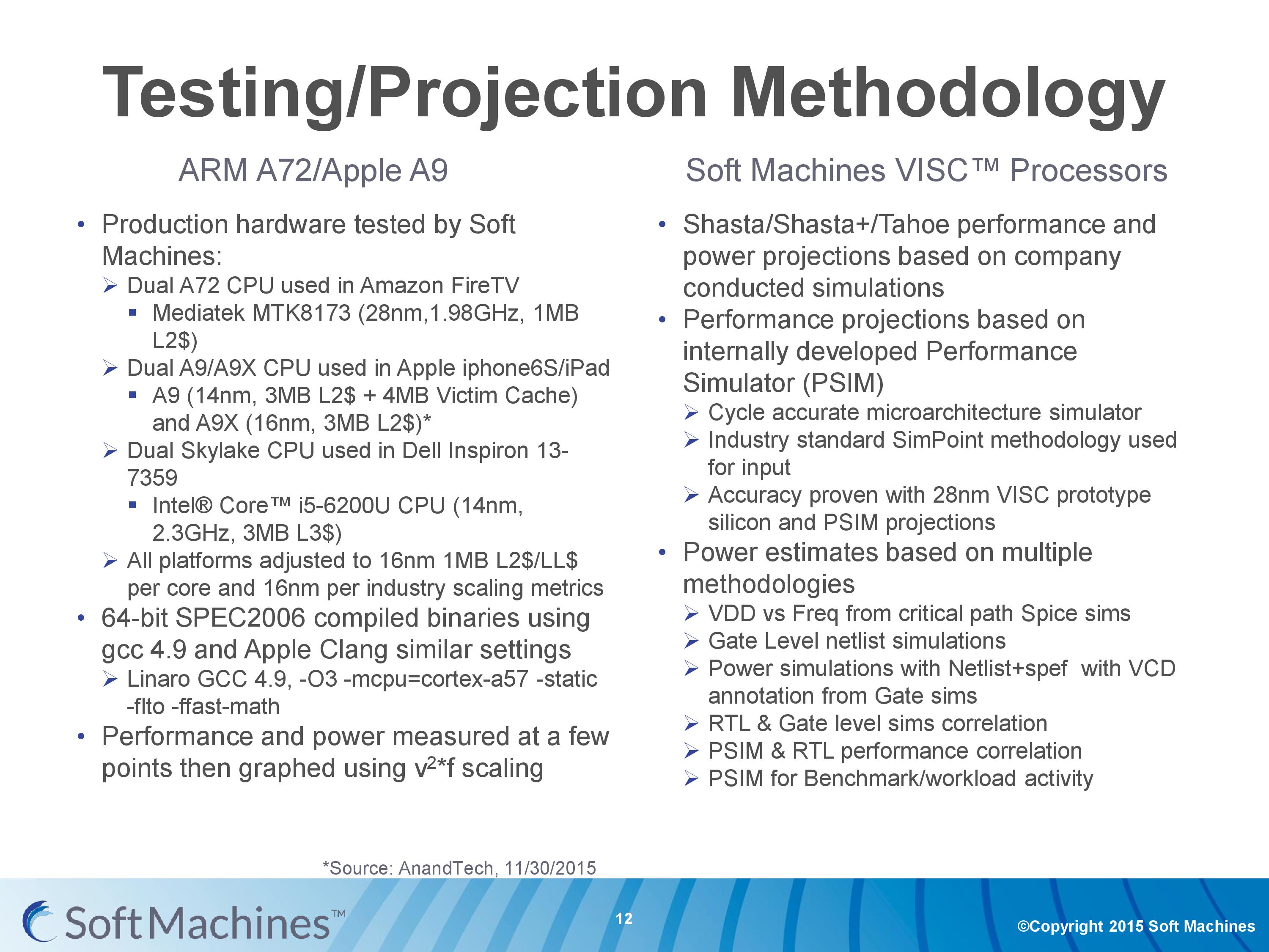
For clarity on the VISC processors, simulations were done to be both signal accurate and cycle accurate, and data taken from 16nm design configurations. Both power and results were taken from these.
For the power on the other parts, the power consumption was taken at the wall. To remove system power from the equation, the system was run in 2C vs 1C modes and 1C vs idle modes at various frequencies to find the dynamic power. Each platform was tested in a cold environment to ensure the maximum temperature did not go above 55C. Each of the power numbers are estimates that have removed the production yield ‘guard’ (i.e. protection overestimate), which was about ~15%, giving benefits to the non-VISC core results.
For the power conversion to 16nm FinFET+ on TSMC:
- The A72 28nm TSMC used TSMC’s numbers for scaling.
- For the A9X numbers, the A9 numbers were taken in a cool environment to minimize Samsung 14nm leakage and the dynamic power for the A9X is assumed the same as the A9.
- For Intel, using public data it was assumed that 16FF+ voltage is 10-15% higher and area is 30% larger, giving ~1.65x power on 16FF+.
- Leakage scales with die area.
For performance testing:
- Linaro GCC 4.9 with -O3 -mcpu=cortex-a57 -static -flto -ffast-math
- If any test failed, results were taken from previous generations and expected percentage increases. For example, FORTRAN on A9 failed, so estimates were taken from the floating point numbers in C.
- For the cache adjustments, for 3MB to 2MB was reduced 3.5-4%. Because Intel has L2+L3, this is reduced a further 5%. For A72 moving from 1MB L2 to 2MB L2 in total, score was increased by 4%.
For a full rundown, this was the slide provided to us:
As part of these assumptions, I did ask about the raw data collected and if that would ever be presented. I did mention that they really need to split up INT and FP results, and I was told that it may happen at a later date but not right now. What I was given though was the effect of the cache adjustment on Skylake.
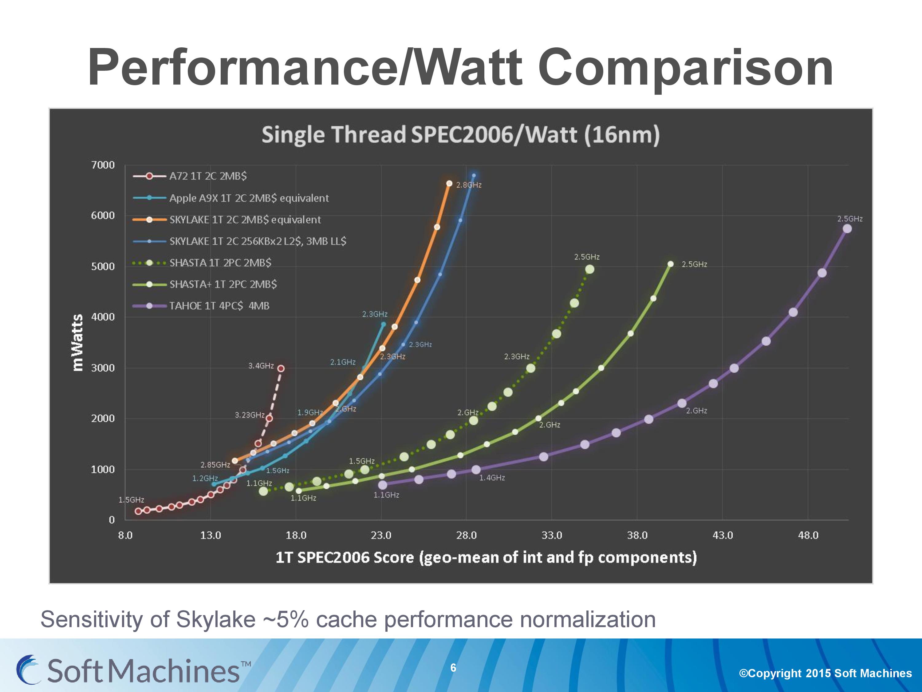
The orange line and the blue line next to it represents the movement from a multi-cache hierarchy of L2+L3 to 1MB of L2 cache per core only. The blue line still has the assumption of moving from 14nm to 16FF+, and using the GCC compiler, but the orange line has that extra assumpton.
Personally, these assumptions make me uneasy. Conversions like this are typically only done as back-of-the-envelope types of calculations during the early stages of design, because they are very rough and do not take into account things like silicon floor-plan optimization that would occur if you chose a smaller/larger cache arrangement, or changing from 8-way to 4-way associativity in the caches and so on. Typically we see companies in similar positions to SMI provide the raw or semi-modified data, using one assumption at most, with a split between FP and INT results - e.g. taking all the results as-is with GCC. The reason why it all comes into one graph is for brief simplicity, which doesn't particularly endear any reader/investor who might decide to be heavily invested in this project.
We pointed out a lot of concerns with this data to Soft Machines, including the list above of assumptions and how some of them simply do not make sense and should be restricted to that those quick rough calculations, especially when presenting at a conference. They gave us the graph above showing the effect of cache changes on Skylake, but I have asked in the future for them to display the data in a less complicated way, using standard industry metrics (such as INT or FP). Ideally the graphs are also kept to two or three data sets without requiring a 9-point interpretation scheme to understand what is happening - we typically get a dozen or so graphs from Huawei, ARM, AMD or Intel when they are describing their latest architecture or microarchitecture designs. This allows more understanding of what is happening under the hood and can be used to validate the results - as it stands, it is difficult to validate anything due to the assumptions and conversions made.


97 Comments
View All Comments
extide - Friday, February 12, 2016 - link
Because a compiler can only schedule instructions to the CPU's front end. This is scheduling of instructions to different ports on the back end of the cpu. The compiler can't tell the CPU what port an instruction goes down, the CPU picks that. THe compiler only gets to pick what instructions are issues, and in what order, and of course, modern CPU's can even change that order if they deem it faster to do so.Exophase - Friday, February 12, 2016 - link
To have any realistic chance of working the threading speculation/detection has to have a large dynamic component (detecting threadlets as they become desirable at runtime) and has to have architectural support for very lightweight thread splitting, merging, and inter-thread communication.That can't be provided by compilers targeting existing instruction sets.
AlexTi - Friday, February 12, 2016 - link
Thanks, I think I got the point finally. This looks similar to what instruction scheduler currently does for execution units in conventional CPU. Virtualization layer + CPUs will be a kind of very wide core. Right?It was already noted in the article, making curent CPU wider is problematic and not universally beneficial. So this new engine should be much more efficient than current implementations.
Good thing is that we'll see eventually :)
Senti - Friday, February 12, 2016 - link
Bullshit. I have no idea how technically incompetent writers should be to reprint that marketing nonsense again and again.First of all, this brings absolutely no advantages over existing fat core + SMT concept. More IPC per core with more pipelines is not done because it's hard to do without that 'virtual cores' nonsense, but simply because there are not enough actually independent instructions that can be automatically extracted from real code during parts where performance matters.
"Alternatively, if multiple programs or threads want to use the hardware, then a single core is inaccessible to additional threads while the first thread is still in use (though this can be avoided somewhat by simultaneous multithreading or SMT which will let another thread have access when the first has encountered a stall such as waiting for L1/L2 memory)." - total lies. That describes coarse-grained multithreading which is not very popular atm. For example, Intel HT allows usually 2 threads to execute simultaneously dynamically sharing pipelines of the same core all the time. POWER8 uses 8 'virtual' threads per core.
Why no one splits instructions from the same thread over several cores (other than the obvious reason that there are not enough independent instructions to split)? Almost quote from the text: "cross-core communication adds latency and reduces performance".
Instruction set emulation? Far from new concept. Why not popular? Reason is very simple: significant overhead. Try translating something non-trivial like AVX/NEON instructions to some generic internal instruction set.
Finally, the last point: everyone can draw cute performance graphs and huge numbers in marketing presentations, but how about giving actually working chips for independent reviews of performance and power efficiency on real code?
vladx - Sunday, February 14, 2016 - link
Skim the article again, there's a roadmap so let's see how things will go from here.Exophase - Friday, February 12, 2016 - link
There's another big question with their power measurements. They take differences between idle and 1C and 1C and 2C to cancel out the static contribution of other peripherals. But this still ignores the dynamic contribution.For example, we can look at Cortex-A72, where ARM claims that one core at 2.5GHz on the TSMC 16FF+ process will consume about 750 mW. In Kirin 950, the power consumption appears to be about 900 mW at 2.3GHz. Is ARM exaggerating or is Huawei's implementation inferior to ARM's expectations? The discrepancy can actually be pretty easily explained by losses in the PMIC/VRMs, the SoC's memory controller, and the DRAM - all components which use more power the more the CPU load increases.
This is especially a factor for wall measurements because they take into effect an additional AC/DC convertor. While it's possible that Soft Machines included these figures in their power estimations I doubt it since they didn't mention it, and like ARM it's more practical and beneficial for them to work with core power estimations only.
So there could easily be another 25+% that the non-VISC platforms are being penalized.
Something else that raises a red flag to me is the 16FF+ test chip. There are only 100 pins. When you take out power, ground, and various control signal are accounted for that leaves a very small interface either to a memory controller or memory (if the controller is integrated). Even a single channel 32-bit interface would be a hard fit. So does this chip really represent both realistic power consumption or realistic performance? I think they're trading one for the other on this one and that makes me question the applicability of the power numbers they've given for it.
Arnulf - Friday, February 12, 2016 - link
Since one cannot buy these "scaled" chips, IMHO it'd make more sense for SMI to publish performance per watt figures of real hardware and let the market decide whether their concept is attractive enough. Yes, Intel may have process node advantage, yes, different CPUs are targetting different performance and power profiles but at least it's a straight comparison and if VISC doesn't beat its entire competition at at least one metric then it's destined to fail anyway.Oh and the remark in the article regarding "VISC advantage" because of it using twice the number of cores while running a single thread in tests - who cares as long as it comes out on top in performance per watt? If they can beat other CPUs by using more cores, kudos to them!
ppi - Saturday, February 13, 2016 - link
Regarding core count, I would direct you to recent AT article on Android usage of multiple cores. Simplified conclusion may be, that Android tends to utilise 4 cores pretty well.In real world, this significantly reduces impact of distributing single thread over multiple cores.
kgardas - Friday, February 12, 2016 - link
Interesting stuff, but to be honest, combining "simpler" cores into more complex is also done by software on SPARC64. At least Fujitsu mentions this on some of their hotchip presentation for SPARC64 VII. So you have 4 cores CPU with 4-wide core and you can combine this by software (compiler) into 8-wide or more depending on your needs for instruction parallelism.Another thing is that something like that is IIRC also supported by POWER8 where you do have a lot of duplicated resources, but not enough so in case 1 thread is able to consume all core resources you may switch-off 7 others. IIRC IBM's compilers contains some optimizations for this too.
Pity think you have mentioned Itanium only in this negative way. Honestly speaking Itanium design was really great and really pity that Intel stopped developing it and not provided any OoO designs on this architecture. If Denver will be successful we will see, but NVidia still counts with it for some designs which may be interesting in a light that they are using ARM's core (A57) for some time now and don't need Denver that much. Also automotive does not care if Denver is there or not yet nVidia pushes it there so I would bet they needs to have really good reason for it. Perhaps their VLIV is good for some special tasks...
So to me whole this looks like they are on another round for money.
Oxford Guy - Friday, February 12, 2016 - link
"Honestly speaking Itanium design was really great and really pity that Intel stopped developing it"The market disagreed so, if you're right, it's a pity the market dictates product success to such a degree.