EUV
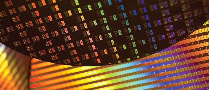
Although TSMC can't claim to be the first fab to use extreme UV (EUV) lithography – that title goes to Samsung – they do get to claim to be the largest. As a result, the company has developed significant experience with EUV over the years, allowing TSMC to refine how they use EUV tooling to both improve productivity/uptime, and to cut down on the costs of using the ultra-fine tools. As part of the company's European Technology Symposium this week, they went into a bit more detail on their EUV usage history, and their progress on further integrating EUV into future process nodes. When TSMC started making chips using EUV lithography in 2019 on its N7+ process (for Huawei's HiSilicon), it held 42% of the...
TSMC: 3nm EUV Development Progress Going Well, Early Customers Engaged
Development of new fabrication technologies never stops at leading-edge companies such as TSMC. Therefore, it is not surprising to hear the annoucement that development of TSMC’s 3nm node is...
76 by Anton Shilov on 7/23/2019
Micron’s DRAM Update: More Capacity, Four More 10nm-Class Nodes, EUV, 64 GB DIMMs
During its earnings conference call with investors and financial analysts earlier this week, Micron expressed confidence in its long-term future and strong demand for its products as new applications...
23 by Anton Shilov on 6/28/2019
Intel Process Technology Update: 10nm Server Products in 1H 2020, Accelerated 7nm in 2021
Intel provided an update regarding its upcoming fabrication technologies at its 2019 Investor Meeting. The company is on track to produce server-class products using its 10 nm manufacturing technology...
74 by Anton Shilov on 5/8/2019
TSMC: No Plans to Buy Rivals at The Moment
Although TSMC expects demand for chips to increase going forward and despite an ongoing trend towards consolidation on the foundry market, the company has commented that it currently has...
4 by Anton Shilov on 4/22/2019
Samsung Completes Development of 5nm EUV Process Technology
Samsung Foundry this week announced that it has completed development of its first-generation 5 nm fabrication process (previously dubbed 5LPE). The manufacturing technology uses extreme ultraviolet lithography (EUVL) and...
21 by Anton Shilov on 4/17/2019
TSMC Reveals 6 nm Process Technology: 7 nm with Higher Transistor Density
TSMC this week unveiled its new 6 nm (CLN6FF, N6) manufacturing technology, which is set to deliver a considerably higher transistor density when compared to the company's 7 nm...
23 by Anton Shilov on 4/17/2019
TSMC’s 5nm EUV Making Progress: PDK, DRM, EDA Tools, 3rd Party IP Ready
TSMC this week has said that it has completed development of tools required for design of SoCs that are made using its 5 nm (CLN5FF, N5) fabrication technology. The...
33 by Anton Shilov on 4/5/2019
SMIC To Start 14nm Mass Production in H1 2019
Reports have emerged this week that SMIC, the largest foundry in China, is set to start mass production using its in-house developed 14 nm FinFET manufacturing technology in the...
20 by Anton Shilov on 2/8/2019
ASML to Ship 30 EUV Scanners in 2019: Faster EUV Tools Coming
ASML said last week that it planned to ship 30 extreme ultraviolet scanners in 2019, up significantly from 2018. The plan is not surprising, as demand for EUV lithography...
17 by Anton Shilov on 1/28/2019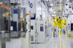
IBM to use Samsung 7nm EUV for Next-Gen POWER and z CPUs
IBM has announced it has signed an agreement with Samsung Foundry to produce its next-generation processors. This includes processors for IBM Power Systems, IBM z, and LinuxONE systems, all...
24 by Anton Shilov on 12/21/2018
Intel: EUV-Enabled 7nm Process Tech is on Track
Originally planned to enter mass production in the second half of 2016, Intel’s 10 nm process technology is still barely used by the company today. Currently the process is...
79 by Anton Shilov on 12/6/2018
Samsung Starts Mass Production of Chips Using Its 7nm EUV Process Tech
Samsung Foundry on Wednesday said that it had started production of chips using its 7LPP manufacturing technology that uses extreme ultraviolet lithography (EUVL) for select layers. The new fabrication...
42 by Billy Tallis & Anton Shilov on 10/17/2018
TSMC: First 7nm EUV Chips Taped Out, 5nm Risk Production in Q2 2019
Last week, TSMC made two important announcements concerning its progress with extreme ultraviolet lithography (EUVL). First up, the company has successfully taped out its first customer chip using its...
50 by Anton Shilov on 10/9/2018
Samsung Foundry Updates: 8LPU Added, EUVL on Track for HVM in 2019
Samsung recently hosted its Samsung Foundry Forum 2018 in Japan, where it made several significant foundry announcements. Besides reiterating plans to start high-volume manufacturing (HVM) using extreme ultraviolet lithography...
29 by Anton Shilov on 9/6/2018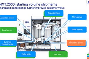
ASML Ships Twinscan NXT:2000i Scanner for 7nm and 5nm DUV
ASML, the company known for producing equipment for the manufacture of processors and semiconductors at foundries, has started to ship its new Twinscan NXT:2000i DUV (Deep Ultra Violet) scanner...
15 by Anton Shilov on 8/2/2018
TSMC Details 5 nm Process Tech: Aggressive Scaling, But Thin Power and Performance Gains
At a special event last week, TSMC announced the first details about its 5 nm manufacturing technology that it plans to use sometime in 2020. CLN5 will be the...
10 by Anton Shilov on 5/8/2018
TSMC Kicks Off Volume Production of 7nm Chips
TSMC last week announced that it had started high volume production (HVM) of chips using their first-gen 7 nm (CLN7FF) process technology. The contract maker of semiconductors says it...
63 by Anton Shilov on 4/24/2018
The Future of Silicon: An Exclusive Interview with Dr. Gary Patton, CTO of GlobalFoundries
In our recent trip to GlobalFoundries Fab 8, its leading edge facility, we managed to spend some time with the C-level executive that controls the future of this part...
39 by Ian Cutress on 2/24/2018
The AnandTech Podcast, Episode 45: GlobalFoundries and Fab 8
In early February, GlobalFoundries did something completely unexpected: for the second time in ten years, they invited a few select press and analysts to visit one of their fabrication...
14 by Ian Cutress on 2/20/2018
TSMC Starts to Build Fab 18: 5 nm, Volume Production in Early 2020
TSMC last week held a groundbreaking ceremony for its Fab 18 phase 1 production facility. The fab will produce chips using TSMC’s 5 nm process starting from early 2020...
27 by Anton Shilov on 1/31/2018


