NVIDIA GeForce GTX 295: Leading the Pack
by Derek Wilson on January 12, 2009 5:15 PM EST- Posted in
- GPUs
Now that we have some hardware in our hands and NVIDIA has formally launched the GeForce GTX 295, we are very interested in putting it to the test. NVIDIA's bid to reclaim the halo is quite an interesting one. If you'll remember from our earlier article on the hardware, the GTX 295 is a dual GPU card that features two chips that combine aspects of the GTX 280 and the GTX 260. The expectation should be that this card will fall between GTX 280 SLI and GTX 260 core 216 SLI.
As for the GTX 295, the GPUs have the TPCs (shader hardware) of the GTX 280 with the memory and pixel power of the GTX 260. This hybrid design gives it lots of shader horsepower with less RAM and raw pixel pushing capability than GTX 280 SLI. This baby should perform better than GTX 260 SLI and slower than GTX 280 SLI. Here are the specs:
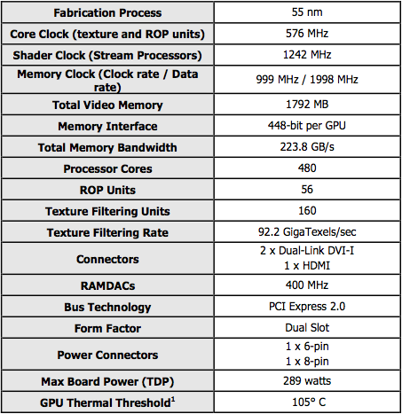
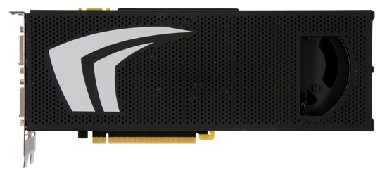
Our card looks the same as the one in the images provided by NVIDIA that we posted in December. It's notable that the GPUs are built at 55nm and are clocked at the speed of a GTX 260 despite having the shader power of the GTX 280 (x2).
We've also got another part coming down the pipe from NVIDIA. The GeForce GTX 285 is a 55nm part that amounts to an overclocked GTX 280. Although we don't have any in house yet, this new card was announced on the 8th and will be available for purchase on the 15th of January 2009.
There isn't much to say on the GeForce GTX 285: it is an overclocked 55nm GTX 280. The clock speeds compare as follows:
| Core Clock Speed (MHz) | Shader Clock Speed (MHz) | Memory Data Rate (MHz) | |
| GTX 280 | 602 | 1296 | 2214 |
| GTX 285 | 648 | 1476 | 2484 |
We don't have performance data for the GTX 285 yet, but expect it (like the GTX 280 and GTX 295) to be necessary only with very large displays.
| GTX 295 | GTX 285 | GTX 280 | GTX 260 Core 216 | GTX 260 | 9800 GTX+ | |
| Stream Processors | 2 x 240 | 240 | 240 | 216 | 192 | 128 |
| Texture Address / Filtering | 2 x 80 / 80 | 80 / 80 | 80 / 80 | 72/72 | 64 / 64 | 64 / 64 |
| ROPs | 28 | 32 | 32 | 28 | 28 | 16 |
| Core Clock | 576MHz | 648MHz | 602MHz | 576MHz | 576MHz | 738MHz |
| Shader Clock | 1242MHz | 1476MHz | 1296MHz | 1242MHz | 1242MHz | 1836MHz |
| Memory Clock | 999MHz | 1242MHz | 1107MHz | 999MHz | 999MHz | 1100MHz |
| Memory Bus Width | 2 x 448-bit | 512-bit | 512-bit | 448-bit | 448-bit | 256-bit |
| Frame Buffer | 2 x 896MB | 1GB | 1GB | 896MB | 896MB | 512MB |
| Transistor Count | 2 x 1.4B | 1.4B | 1.4B | 1.4B | 1.4B | 754M |
| Manufacturing Process | TSMC 55nm | TSMC 55nm | TSMC 65nm | TSMC 65nm | TSMC 65nm | TSMC 55nm |
| Price Point | $500 | $??? | $350 - $400 | $250 - $300 | $250 - $300 | $150 - 200 |
For this article will focus heavily on the performance of the GeForce GTX 295, as we've already covered the basic architecture and specifications. We will recap them and cover the card itself on the next page, but for more detail see our initial article on the subject.
The Test
| Test Setup | |
| CPU | Intel Core i7-965 3.2GHz |
| Motherboard | ASUS Rampage II Extreme X58 |
| Video Cards | ATI Radeon HD 4870 X2 ATI Radeon HD 4870 1GB NVIDIA GeForce GTX 295 NVIDIA GeForce GTX 280 SLI NVIDIA GeForce GTX 260 SLI NVIDIA GeForce GTX 280 NVIDIA GeForce GTX 260 |
| Video Drivers | Catalyst 8.12 hotfix ForceWare 181.20 |
| Hard Drive | Intel X25-M 80GB SSD |
| RAM | 6 x 1GB DDR3-1066 7-7-7-20 |
| Operating System | Windows Vista Ultimate 64-bit SP1 |
| PSU | PC Power & Cooling Turbo Cool 1200W |


100 Comments
View All Comments
LinkedKube - Tuesday, January 20, 2009 - link
I am not a fan boy of any kind. I recently considered buying a 4870x2, until I heard about the 295, which I will be purchasing soon.The article was a bore, as I currently own a g80 ultra, and still regret paying the 750usd for it a year and a half ago.
I'm currently thanking the situation of competing card markers because I dont have to go through the high end cards looking at a 750~ price range of cards. It was the best card at the time, and that's what I bought, if ati would have had a better card I'd own an ati xxxx w/e it may have been.
If you're willing to spend 400usd+ on a card, power consumption shouldnt be an issue to argue about.
This is two 280's slapped together, we all know that, yes its the best card currently. Is it worth the money? Probably not if you have bills to pay and have fears of feeding yourself afterwards.
To each his own though. It looks like this silicon guy has about 7 months worth of ati hate in his blood. I'm wondering if he has a black and green case to go along with his nvidia "aura."
rocky1234 - Monday, January 19, 2009 - link
First off this was a pretty good article it shows that Nvidia finally has a card that can topple the mighty ATI card in some of the tests but not all. Keep up the good work.I also own a ATI 4870x2 card it works great have not had any problems with it as of yet except for minor driver issues with crossfire in 2 games but those were worked out. I used to own only nvidia but got tired of their lame assed renaming of old product to a newer higher number then try to fool people into buying these new cards. I still own a 8800/9800GT card & it will be the last nvidia card I buy for awhile until they decide to stop trying to screw people over by rehashing the old cards as new cards. This geforce 295 does look like a good card but for the small amount it gives over a 4870x2 card I think I will wait for the next gen of cards to come out before I spend money again on a new card.
oh yeah to SiliconDoc no need to point out any spelling mistakes or missed periods here & there as I don't really care what you got to say you proved over & over again you are a nvidia fanboy & really have nothing usefull to say that we all already didn't know. its nothing personal but until you take your head out of your butt & wake up & smell the daisy's we just don't care. Also no need to reply to this as I won't care to reply to what you got to say SiliconDoc. I only singled you out because you attacked so many people in this thread only because they had personal views to express.
enough said
rocky1234
chuouwee - Thursday, January 15, 2009 - link
Imo... the 295 seems like it only avgs around 5-6 fps than the 4870 x2 overall the games reviewed in this article... I don't think it justifies the extra 50-100 dollars we would be spending on the card...SiliconDoc - Saturday, January 17, 2009 - link
I think the combination of that, along with CUDA, the PsysX factor, the ability for instant use in the supplied driver on the CD that comes with the card GAMING Profiles, AND to use your 8 series and above card as a PhysX processor in another pci-e slot, EASILY makes up for price differences. Not to mention the 60 watts in idle and 45 watts in 3d power $avings the GTX295 offers over the 4870x2...When you add it all up - IT'S VERY CLEAR WHY THERE ARE PRICE DIFFERENCES AND WHY THE ATI CARD IS DROPPING LIKE A ROCK.
Hrel - Tuesday, January 13, 2009 - link
Can you PLEASE! start including 3DMark numbers in your GPU reviews? PLEASE!san1s - Tuesday, January 13, 2009 - link
can you please tell me how to "play" 3dmark?It must be so fun watching the same scene being rendered on your screen over and over again
kzVegas - Tuesday, January 13, 2009 - link
It seems that nearly every author at Anandtech has been told to view nVidia product's with the same enthusiasm as looking for dimes in a well used cat box. The author of this article brackets his test of the GTX295 with two tests of games that are not very popular just to show that an AMD/ATI card can best the nVidia offering. Then goes on to argue in his closing comments that AMD needs to do better with its drivers. The points out this card is $50 more than a cheap 4870x2 and thats %10 more expensive. WHO CARES? When someone is going to spend $450 to $500 for a card the difference in price isn't all that important. I'd like to see more articles that don't appear to be so biased against one company or the other.strikeback03 - Wednesday, January 14, 2009 - link
I always love the bias comments after every graphics card review, because no matter what hardware is being reviewed or what they thought of it somebody will claim they are biased. Go check the comments after pretty much any AMD GPU review - there will be at least one person (and usually several) complaining because they spent too many words in the article talking about the nVidia competition and which is better at what price, with no "This is the best card EVAR!1!" endorsement.Anandtech crew, thanks for all your work!
SiliconDoc - Saturday, January 17, 2009 - link
Now show me in the 4870x2 review where a 30" monitor is described as the very neccessity of purchase...I checked there is one line buried between two others that mentions resolution needs...
I could care less what IDIOTS state in comments as "your proof" that people complain about bias from "both sides".
Unless you address the SPECIFIC POINTS of any one complaint be REFUTING THEIR CONTENT WITH THE ARTICLES OWN WORDS ...
you have failed.
It's not my fault you're lazy in that regard, and would rather just whine there is no bias (because of opposinbg complaints) and then spew your anand praise points as your infantile final analysis.
I ADRESSED a half dozen and more bias issues in my posts here, and you completely ignored every single one of them - in favor of " there are complaints from either quarter".
Address this then, mister even steven - in these posts we have a good number of cussing raging redfans spewing death toward my and a few others posts - who pointed out redcard issues. We don't see that going the other way, here, AT ALL.
Now, who then is raging, cussing, spewing monkey set of fan bias ?
Take a look and read the postings.
One commenter even spammed his response to me, like half a dozen times.
No matter HOW MUCH you claim it to be true, we do NOT see that type of beghavior going the other way - green fans wishing death upon the red suporters. I have never seen it in fact, at dozens of review comment sites.
Have you ? Would you like to look ?
Once again, the easiest way out is whining there are both types, and therefore neither is correct.
The problem is, I have not been constantly lying and exagerrating, and twisting the truth, I have been the one correcting the lies and shenanigans. There is a difference, and you'd know it if you cared to notice.
Now refute any of my arguments in this entire thread from any of my posts, I'm WAITING MR FAIR !
If you refite most of them, why then you've proven your point, huh.
Otherwise, you're a bag of lying wind.
SiliconDoc - Thursday, January 15, 2009 - link
I read the entire 4870x2 review before saying what I did. Of course you didn't do the same.