nForce2 6-way Motherboard Roundup - December 2002
by Evan Lieb on December 4, 2002 6:53 PM EST- Posted in
- Motherboards
ASUS A7N8X: BIOS and Overclocking
ASUS has always used their own unique BIOS format, though the A7N8X BIOS is still based on Phoenix Technology's Award BIOS.
There is a good deal of readings available in the A7N8X Hardware Monitor portion of the BIOS.
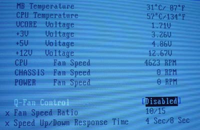
These readings include CPU and motherboard temperatures, Vcore, PSU readings (all rails), three different fan speed readings (CPU, chassis, power), and ASUS's very own patented Q-fan control, which regulates your CPU fan speed based on how taxed your system is at any given moment. These are fairly basic readings for a high-performance BIOS, but it's quite acceptable nonetheless.
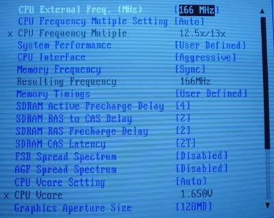
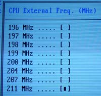
The Advanced Chipset Features section includes a fair amount of options. These include adjustments for FSB (up to 211MHz), CPU multiplier, memory frequency, various memory timings, Vcore, VAGP, and VDIMM. The picture above doesn't show the VAGP or VDIMM adjustments, but they're certainly there.
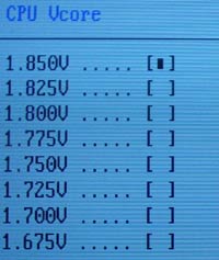
The A7N8X BIOS has some fairly decent voltage tweaking capability.
First off, Vcore is adjustable in .025V increments all the way up to 1.85V.
Like the NF7-S, this is pretty low for Palomino users, but we suggest you
use a Thoroughbred-B processor anyway, as a 0.2V increase in Vcore should
be more than enough for avid Thoroughbred overclockers. Running any higher
than 1.85V really isn't recommended, even with heavy-duty cooling setups.
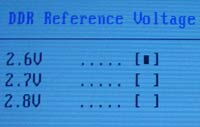
In the A7N8X BIOS you're able to adjust VDIMM up to 2.8V in 0.1V increments. Memory overclockers shouldn't have any trouble with this type of memory voltage availability, especially since we were able to get a decent memory overclock with VDIMM set at just 2.6V.
The A7N8X BIOS definitely does contain an AGP bus lock at 66MHz. However, what about the PCI bus lock at 33MHz? For this question we headed over to ASUS and asked them what was going on. ASUS's response was simply that they have a PCI bus lock set at 33MHz and that you have nothing to worry about as far as running your devices out of specification while performing FSB overclocking.
Overclocking the ASUS A7N8X Deluxe was very easy for the most part. Here were our FSB overclocking results using the following setup:
|
Front Side Bus Overclocking Testbed |
|
|
Processor:
|
Athlon
XP 2400+
|
|
CPU
Vcore:
|
1.65V
|
|
Cooling:
|
AMD
Retail HSF & Thermal Pad
|
|
Power
Supply:
|
Enermax
300W
|
We were able to reach 185MHz FSB (370MHz DDR) using this conservative overclocking setup. This overclocked FSB frequency is normal compared to the other nForce2 SPP motherboards we've tested here today.
Using a factory locked Athlon XP 2400+ processor, all we had to do was simply lower the CPU multiplier down to 8X and increase the FSB as high as we possibly could without jeopardizing stability and without increasing voltages. This was made possible by a great feature the ASUS A7N8X Deluxe affords (as do all nForce2 motherboards), and that's the ability to adjust the CPU multiplier in the BIOS without having to do physical modification to the CPU. Therefore, all you have to do is install your multiplier-locked Athlon XP CPU into your nForce2 motherboard and voila; you can adjust all the available multipliers to your heart's content. However, make sure you purchase the right type of Athlon XP; only Thoroughbred-B processors have this capability on nForce2 motherboards. You cannot change the multiplier of a locked Palomino or Thoroughbred-A processor in any of the six nForce2 motherboards being reviewed today.
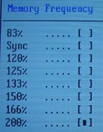
There also are lots of divider options available, exactly the same ones you'll see in most nForce2 BIOSes. You can adjust memory in many different ways, and as high as 400MHz if you'd really like to. See the above picture for more info.


1 Comments
View All Comments
c627627 - Monday, July 21, 2003 - link
MSI contradicts your reviewhttp://www.anandtech.com/mb/showdoc.html?i=1759&am...
You say:
"12/04/02 UPDATE: MSI sends word that the K7N2-L indeed does not have a PCI bus lock at 33MHz."
To this day, that was used as ultimate proof that the original MSI nForce2 mobo does not have a PCI lock.
Today MSI Senior Moderators said:
"they are wrong,and who ever told them it did not from msi"
(!)
Source:
http://www.msi.com.tw/program/e_service/forum/thre...
Won't you please settle this for us.