NVIDIA GeForce3 Investigation: What NVIDIA didn't tell us
by Kert Chian on May 15, 2001 1:18 AM EST- Posted in
- GPUs
What didn't NVIDIA tell us about their latest creation? Hopefully, you will find the answers at the end of this article. This article sets out to unravel the secrets held within the little black box that is the GeForce3. As a matter of fact, quite a few of these nuggets of information are publicly available but require patience in sifting through the noise and funny names; others from running benchmarks on an 850 MHz Athlon Thunderbird at a dozen different settings day in and day out, swapping a GeForce2 Ultra with a GeForce3 using the latest drivers (Driver version: 4.13.01.1210). Still others come under the section of industrial secrets. The GeForce3's depth buffer optimizations (Z-compression, Z-occlusion culling and Crossbar memory controller) belong to this category.
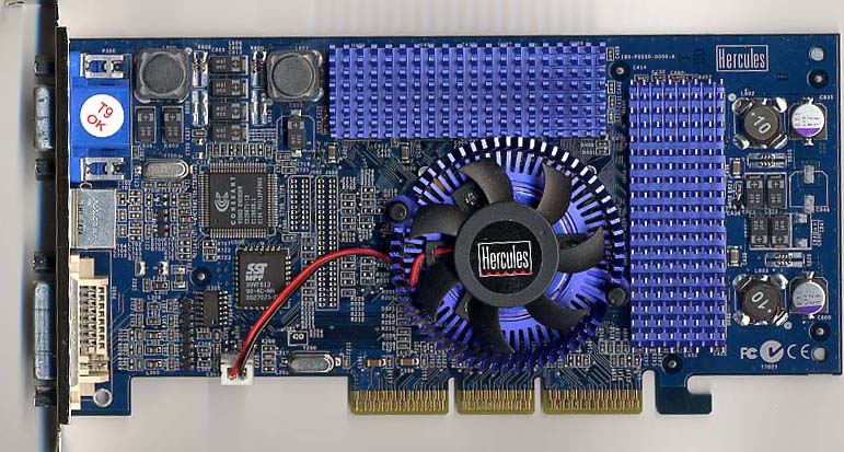
A Hercules GeForce3
This review isn't intended to be a large comparison of cards, rather it was designed to focus on some of the technologies behind the 57 million transistor GeForce3 core. We suggest that you take a look at our first two reviews of the GeForce3 (Architecture Overview and Performance Review) before proceeding with this one.
The Test
|
Windows 98 SE Test System |
|||||||
|
Hardware |
|||||||
| CPU(s) | AMD Athlon-B (Thunderbird) 850MHz (100MHz DDR FSB) | ||||||
| Motherboard(s) | ASUS A7V133 | ||||||
| Memory | 256MB PC133 Hyundai SDRAM | ||||||
| Hard Drive |
Seagate Barracuda 20GB 7200RPM Ultra ATA 66 |
||||||
| CDROM |
Acer 24X |
||||||
| Video Card(s) |
NVIDIA GeForce2 Ultra 64MB DDR (clocked at 200/230 - core/mem) |
||||||
| Ethernet |
N/A |
||||||
|
Software |
|||||||
|
Operating System |
Windows 98 |
||||||
| Video Drivers |
|
||||||
Note: The GeForce2 Ultra was clocked at a 200MHz core instead of 250MHz to provide for a better tool in our analysis of the GeForce3's advantages.


0 Comments
View All Comments