Intel Demonstrates new 45nm Transistors and Conroe's Successor
by Anand Lal Shimpi on January 27, 2007 12:00 AM EST- Posted in
- CPUs
They often say that the bigger a company gets, the more difficult it is to make sweeping changes to fix problems. Analogous to quickly turning a small boat vs. a large tanker, no one would have ever expected Intel to change so quickly over the past several months.
It's not only on the performance side that we've seen tremendous change; after all, it just took a new architecture to do that. No, the change we're speaking of here is in how Intel conducts itself, how freely it shares information today and how very different the road to 45nm has been compared to the move to 90nm or 65nm.
Today Intel is announcing a number of details on its 45nm process node, including official details on the first family of 45nm processors due out later this year. The announcements themselves, as you will soon see, are impressive enough, but arguably more interesting is the amount of detail Intel is giving away at this point. In the past we've had to go to sources other than official Intel channels for this sort of information, but that has all changed with the new Intel.
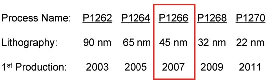
On track for first production by the end of 2007 with the Penryn family of processors (mobile, desktop and server), is Intel's 45nm manufacturing process. As with any move to smaller transistors, the 45nm node will make chips smaller and run faster. Intel is actually seeing good feature scaling with its 45nm process, quoting a ~2x improvement in transistor density. In other words, if you took a 100mm^2 65nm chip and built it on Intel's 45nm process, it would be roughly a 50mm^2 chip after the shrink. While logic and cache structures generally end up scaling very well with a process shrink, I/O structures (e.g. main memory interface circuits) don't which is why the improvement in transistor density is roughly and not exactly 2x.
Of course, in the past Intel has usually coupled new process technology with more features so you shouldn't expect to see 45nm Penryn chips as simply smaller Core 2 Duos. We will look at Penryn's die in a moment, but a larger cache, SSE4 and other unannounced microarchitectural enhancements can be expected.
The story of Intel's 45nm process doesn't end with details on its feature scaling however. Intel has made some fairly significant changes to the transistors themselves that make them more efficient than normal.


59 Comments
View All Comments
quidpro - Monday, February 26, 2007 - link
What is Glaze? google is not helping.Hoser McMoose - Wednesday, January 31, 2007 - link
The calculation for the number of transistors for cache is off by a fairly significant amount in this article! The article states 288M transistors for 6MB of cache, which is FAR too low!Actual transistors for 6MB cache, if we assume ZERO redundancy is:
6MB * 1024KB/MB * 1024B/KB = 6,291,456 bytes
6,291,456 bytes * 9 bits/byte = 56,623,104 bits (remember ECC makes it 9 bits, not 8)
56,623,104 bits * 6 bits/transistor ~= 340M transistors
In reality it is actually probably more like 350 or 360M transistors required for 6MB of L2 cache since you always want a bit of redundancy. It's a bad thing if you have to throw out an entire chip due to a single bit error in your 6MB of cache!
Now, taking those numbers, if we assume that the 410M Transistor figure is accurate, the change in transistors from Conroe to Penryn is a bit different.
Conroe has 291M transistors of which at least 226M are L2 cache. That leaves only 65M assuming no redundancy, or maybe more like 50M transistors with a few redundant cache cells. According to www.sandpile.org (and I have no idea what their source is) each core of the Core 2 Duo has only 19M logic transistors. If this is accurate then it's actually HUGELY impressive, since that is WAY less then either the Pentium 4 or the Athlon64.
Murst - Monday, January 29, 2007 - link
"Intel isn't disclosing how thick the Hafnium gate dielectric layer is in its 45nm transistors, but we do know that it is thicker than the 1.2nm SiO2 gate dielectric used in previous 90nm and 65nm transistors."Why would intel make the gate larger in a shrink? Is this a typo, or is there some huge benefit to this?
IntelUser2000 - Tuesday, January 30, 2007 - link
The reason is that making the gate dielectric thinner than 1.2nm is not a good idea. 1.2nm dielectric is already equivalent to 5 atoms in thickness. Electrons can literally squeeze through the dielectric "insulator" because the dielectric is so thin. Because the material used for the dielectric layer is different from the 65nm generation, they can make the dielectric thicker without sacrificing speed characteristics. So they can increase speed AND have substantially less leakage.
Visual - Monday, January 29, 2007 - link
So, I'm a bit out of the loop lately, can anyone brief me up?Are there any new sockets, chipsets, ram changes or anything expected together with these new 45nm goodies? Or will I be fine getting a new system come Q2, and upgrading to Penryn when it's out and affordable?
ceefka - Monday, January 29, 2007 - link
I wonder if booting OXS with the new chip indicates that PC-users can soon use OSX too without having to buy a Mac. That would allow to mix and match a bit more with apps.Netopia - Sunday, January 28, 2007 - link
100 * 100 =10,000
50 * 50 = 2,500
That's a 4x improvement, not a 2x!
Joe
coldpower27 - Sunday, January 28, 2007 - link
That is not how it works...65 x 65 = 4225
45 x 45 = 2025
2025/4225 = 48% the size of the 65nm part, so close to 2x smaller.
IntelUser2000 - Sunday, January 28, 2007 - link
That's the theory. Intel's 45nm 6T SRAM size is 0.346um, and 65nm SRAM cell size is 0.57um. That's only 39% reduction(61% of the size). In addition, SRAM, which is used for cache, has the best potential for scaling. The cores will have likely worse scaling than 61%.
coldpower27 - Monday, January 29, 2007 - link
Yes, I was just presenting the mathematical example of the calculation, I wasn't going into having real world factors involved. Since in this article Anandtech simplified things with just the 2x smaller statement.