Intel's 0.09-micron Process - More Details Emerge
by Anand Lal Shimpi on August 13, 2002 4:02 AM EST- Posted in
- CPUs
A Very Cache-Friendly Process
One of Intel's biggest accomplishments with their 90nm process is an incredibly high cache density. In their March announcement, Intel introduced the world's highest capacity SRAM chip (6.5MB) on this 90nm process and its significance extends far beyond bragging rights.
 |
 |
|
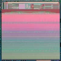
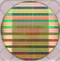
A 52Mbit SRAM chip manufactured on Intel's 90nm process (left). All parts built on Intel's 90nm process will be built on 300mm/12" wafers. This wafer of 90nm chips is composed of 330 billion transistors (right). |
|
As we mentioned before, Prescott will be home to a 1MB L2 cache, which is very impressive for a desktop chip. It wasn't too long ago that 1MB caches were reserved to server chips alone, but with their 90nm process Intel will be able to bring large L2 caches to the desktop. And they will need to in order to offer performance competitive to AMD's Hammer; with the Hammer's on-die memory controller, memory accesses can happen much faster meaning that the more often Prescott has to go to memory to fetch data, the more often Hammer will be faster in comparison. Having a very large L2 cache reduces the frequency Prescott will have to go to main memory for most applications without resorting to an on-die memory controller.
If Intel's desktop chips will get a 1MB L2 cache, what about their server solutions? It has been well known that Intel's Madison processor (third generation derivative of Itanium) would have a massive 6MB on-die L3 cache on a 0.13-micron process, but armed with Intel's 90nm process the Montecito core (fourth generation Itanium) will boast an incredible 12MB on-die L3 cache using close to 800 million of these 90nm transistors.
But being able to put larger caches on-die while taking up as little space as possible is just one of the feathers in Intel's 90nm cap…


0 Comments
View All Comments