ATI’s Radeon 9700 (R300) – Crowning the New King
by Anand Lal Shimpi on July 18, 2002 5:00 AM EST- Posted in
- GPUs
The Chip behind the Name
As we originally hypothesized back at Computex, the R300 is a 0.15-micron chip but it is also fully DirectX 9 compliant. Being DirectX 9 compliant means that the R300 pipeline is fully floating point from start to finish, which increases the transistor count of the chip tremendously. The combination of a fully floating point pipeline and features such as the chip’s 8 rendering pipelines give the R300 a transistor count of over 110 million transistors. While this is less than what we’re estimating for NV30, it’s definitely higher than any currently available GPU. Note that the Matrox Parhelia is an 80M transistor chip, also manufactured on a 0.15-micron process.
One of the problems associated with having this many transistors on a 0.15-micron chip is that the chip will inevitably be extremely large; this poses two problems, packaging and yield.
The R300 chip itself has over 1,000 pins, more than AMD’s forthcoming ClawHammer CPU. Part of the reason for the increase in pin count is the move to a 256-bit memory bus, but a good number of those pins are power delivery pins to feed the massive chip. Because of the incredible pincount of the chip, ATI is the first to use a Flip-Chip package (FCBGA) for a GPU with the R300.
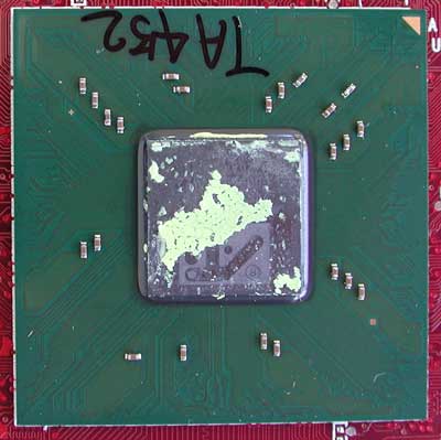
As you can see from the picture above, the R300 looks a lot like a modern-day CPU like the Pentium 3, Pentium 4 (without the heatspreader) or Athlon XP. The benefits of a FC-BGA package include the ability to route 1,000+ pins properly as well as improved cooling, which is definitely necessary for such a complex chip running at such high clock speeds.
The next problem you run into with such a complex chip is this issue of yield; in order for the R300 to be competitive, clock speeds would have to be at least equal to that of the GeForce4. NVIDIA was able to hit 300MHz on their 0.15-micron process, but that was for a 63M transistor chip. The transistor count is almost double with the R300, yet ATI was shooting for greater than 300MHz.
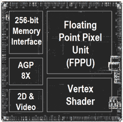
The R300 die, note the large amount taken up by the FPPU.
According to one of ATI’s chip architects, the reason they were able to reach such high clock speeds when 3DLabs and Matrox were unable to go much beyond 200MHz was because they took a different approach to the chip design. An admittedly very “Intel-like” approach, ATI didn’t go as far as to hand pick transistors but they did a considerable amount of the R300 design by hand thus enabling them to reach decent clock speeds at profitable yields.


0 Comments
View All Comments