ATI Gives Chipsets a Try - Introducing the Radeon IGP
by Anand Lal Shimpi on March 13, 2002 12:07 PM EST- Posted in
- CPUs
It takes two
As with all of today's desktop chipsets, the ATI Radeon IGP chipset is composed of two chips, effectively a North and a South Bridge. The equivalent of the North Bridge is actually called the ATI Radeon IGP (Integrated Graphics Processor) which also happens to be the name of the chipset family as well.
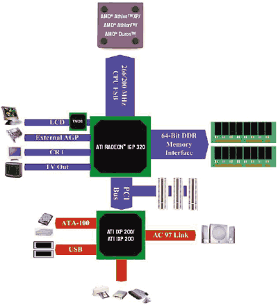
The Radeon IGP 320 will be used in Athlon systems
From a pure North Bridge perspective, ATI's Radeon IGP is nothing special. ATI does have licenses for both the Athlon's bus and the Pentium 4's bus so you will see one or the other supported in various Radeon IGPs (we'll get into the various model numbers later). The Radeon IGP features a single channel 64-bit DDR memory controller supporting either DDR200 or DDR266 SDRAM. While there is thought about supporting DDR333 that will be decided upon in the future but for now those two frequencies are it.
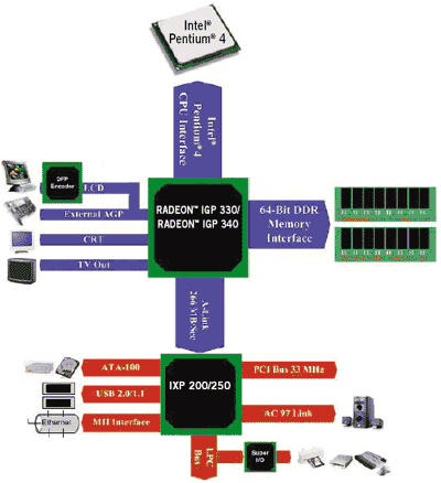
The Radeon IGP 330/340 will be used in Pentium 4 systems as well
The Radeon IGP has a 32-bit/33MHz point-to-point link that ATI calls their A-Link to connect to ATI's own South Bridge. This link is also designed in such a way that it is backwards compatible with 32-bit/33MHz PCI links meaning that the Radeon IGP can be used with a number of currently available South Bridges such as the VIA 686B.
Finally the Radeon IGP also features a connection to an AGP 4X port, rounding it out as your run-of-the-mill North Bridge.
 The
biggest selling point of the Radeon IGP however is its integrated graphics which
ATI promises will be leaps and bounds better than anything out there currently
(with the exception of the nForce). The integrated graphics is based on the
Radeon VE core which means that it has no Hardware T&L support, only a single
rendering pipeline, and the ability to output three texels per clock. On the
up-side this also means that the integrated graphics features HydraVision, ATI's
excellent hardware accelerated DVD playback (with iDCT and hardware motion compensation
support), and HyperZ. ATI's PowerPlay power saving technology is also included
in the Radeon IGP which makes a lot of sense for the mobile application of the
chipset (more on that later as well). The current IGP also lacks any integrated
TMDS transmitter which makes sense for the target market of the Radeon IGP.
The
biggest selling point of the Radeon IGP however is its integrated graphics which
ATI promises will be leaps and bounds better than anything out there currently
(with the exception of the nForce). The integrated graphics is based on the
Radeon VE core which means that it has no Hardware T&L support, only a single
rendering pipeline, and the ability to output three texels per clock. On the
up-side this also means that the integrated graphics features HydraVision, ATI's
excellent hardware accelerated DVD playback (with iDCT and hardware motion compensation
support), and HyperZ. ATI's PowerPlay power saving technology is also included
in the Radeon IGP which makes a lot of sense for the mobile application of the
chipset (more on that later as well). The current IGP also lacks any integrated
TMDS transmitter which makes sense for the target market of the Radeon IGP.
The integrated graphics core will eventually get a performance/feature bump as ATI does realize that the Radeon VE core isn't the most attractive, even if you're not too concerned with performance. By the end of this year or maybe into early 2003 ATI hopes to have a version of the Radeon IGP with a Radeon 8500 derived graphics core and in late 2003/early 2004 ATI expects to have their next-generation core integrated into their IGP product. This should give you an idea of what to expect from ATI on the chipset side of things, basically a single release every year.
By using a very small integrated graphics core and sticking to only a 64-bit DDR memory controller ATI is able to price the Radeon IGP competitively with solutions from ALi, SiS and VIA. This also means that the performance of the overall solution will definitely suffer as a result of a limited amount of memory bandwidth, remember that the 2.1GB/s provided by a 64-bit DDR266 bus must now be shared between the CPU and the integrated graphics core.


0 Comments
View All Comments