Huawei Honor 6 Review
by Andrei Frumusanu & Joshua Ho on September 12, 2014 9:00 AM EST- Posted in
- Smartphones
- Huawei
- Android
- Mobile
- Honor 6
Kirin 920 SoC & Platform Power Analysis
The central point of the Honor 6 is the new HiSilicon Kirin 920. This is the first non-Samsung big.LITTLE chip that managed to get to market in consumer devices. The Kirin 920 is the successor to HiSIlicon's Kirin 910T that is shipping with the Huawei Ascend P7, but don't let the minor naming scheme change fool you as the 920, or more aptly, the Hi3630 as its actual model number describes it, is a major generational upgrade in every measurable aspect.
The Hi3630 is a fully HMP-enabled big.LITTLE design with 4x Cortex A7 and 4x Cortex A15 cores. HiSilicon has remained relatively conservative with the clock speeds and as such we don't see them exceeding 1.3 and respectively 1.7GHz for the little and big clusters. We see implementation of newer r3 A15 silicon IP for the big CPUs and should expect better power management and power efficiency as opposed to past A15 implementations.
On the GPU side we find a Mali T628MP4 clocked in at 600MHz. This is nothing to write home about as the T628 was to be found in devices already over a year ago in the form of the Exynos 5420. The MP4 configuration is also a downgrade from Samsung's MP6 implementation, so we should expect lower performance. I feel a bit underwhelmed by HiSilicon's GPU decision here as it seems they target a more mid-range performance segment rather than trying to compete with Samsung and Qualcomm. We'll see later in the benchmark section how this works out for the Honor 6.
| HiSilicon "Kirin 920" Hi3630 vs Direct Competitors | ||||
| SoC | HiSilicon Hi3630 |
Samsung Exynos 5422 |
Samsung Exynos 5430 |
Qualcomm MSM8974v3 |
| CPU | 4x Cortex A7 r0p5 @ 1.3GHz + 4x Cortex A15 r3p3 @ 1.7GHz |
4x Cortex A7 r0p5 @ 1.3GHz + 4x Cortex A15 r2p4 @ 1.9GHz |
4x Cortex A7 r0p5 @ 1.3GHz + 4x Cortex A15 r3p3 @ 1.8GHz |
4x Krait 400 @ 2.3GHz |
| Memory Controller |
2x 32-bit @ 800MHz DDR 12.8GB/s b/w |
2x 32-bit @ 933MHz DDR 14.9GB/s b/w |
2x 32-bit @ 1066MHz DDR 17.0GB/s b/w |
2x 32-bit @ 933MHz DDR 14.9GB/s b/w |
| GPU | Mali T628MP4 @ 600MHz |
Mali T628MP6 @ 533MHz |
Mali T628MP6 @ 600MHz |
Adreno 330 @ 578MHz |
| Integrated Modem |
"Balong" LTE Cat. 6 300Mbps |
n/a | n/a | MDM 9x25 LTE Cat. 4 150MBps |
| Video H/W |
H264 1080p Enc- & Decoder |
H264 2160p Enc- & Decoder |
H264 2160p Enc- & Decoder + H265 4K Decoder |
H264 2160p Enc- & Decoder |
| Mfc. Process |
TSMC 28nm HPm |
Samsung 28nm HKMG |
Samsung 20nm HKMG |
TSMC 28nm HPm |
The SoC is manufactured on TSMC's 28nm HPm process. Unfortunately I wasn't able to determine the running voltages of the chip as it seems HiSilicon employs a separate microcontroller and closed firmware layer for direct DVFS controlling (DVFS is still arbitrated by the kernel though).
We have a standard 2x32bit LPDDR3 memory interface running at 800MHz DDR, making available some 12.8GB/s of bandwidth to the SoC. Hardware video encoder and decoders allow for H264 1080p recording and playback. The SoC employs some auxillary accelerator blocks such as a JPEG hardware unit. We have little information on the ISP that HiSilicon employs but it should be of a similar design as Samsung employs, meaning a Cortex A5 core with dedicated SIMD accelerators.
The NAND/MMC interfaces use the same DesignWare IP that we find on Exynos SoCs, deploying 3 controllers each handling the main eMMC NAND, the external SD card via SDIO, and also the Broadcom BCM4334 Wi-Fi chip via SDIO.
Probably the most important aspect of the Kirin 920 SoC is that it has a new integrated LTE modem built into the same die. The "Balong" modem is capable of category 6 LTE speeds with carrier aggregation, not only making this one among the first Cat. 6 modems, but the very first integrated silicon available from any vendor. Looking back at the rest of the SoC's specifications this might have been one of the reasons as to why the SoC appears to have conservative specifications, as modems take a long time to validate and having it integrated into a SoC also delays the whole chip.
Unfortunately we couldn't review the modem in this Chinese unit as it lacks the RF front-end compatible with western FDD networks. For what it's worth, it runs 2G and EDGE seemingly well...
Power management
While knowing about the silicon employed gives us some notion about its expected performance, nowdays modern power management makes it pretty much unpredictable as to how efficient a SoC will be. In the future I'll be trying to expose more of how vendors implement their power management schemes and what we should expect of devices in daily use.
In the case of the HiSilicon Hi3630 there's a bit of a double-edged sword story going on.
As a fully HMP-enabled big.LITTLE chip, the OS employs a full Global Task Scheduling (GTS) scheme inside of the Linux Kernel (version 3.10.33) on the device. To be able to understand GTS we need a little explanation around the core mechanism which decides how a task is migrated between the two clusters:
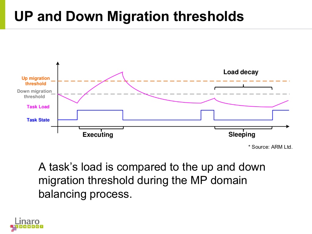
The kernel employs a mechanism to track load continously for each scheduler entity (a process or a cgroup of processes). This per-entity load-racking algorithm is at the core of the scheduler mechanic for GTS. A simplified overview defines three main control parameters: the up- and down-thresholds and the load-average period which acts as a window frame for the decision making. If a task's load exceeds the up-threshold, it is migrated over to the big cluster, and similarly if the task's load falls under the down-threshold it bounced back onto the little cluster.
In Huawei's case we see the use of the HMP up- and down- as variable control parameters as the prefered method to control performance and power of the chip as opposed to the usual clock-frequency limits. Keep this in mind for the battery life benchmarks as this will impact them in substantial ways.
The chip comes of course will advanced clock- and power-gating mechanisms for the CPU cores. We have the usual ARM architectural core clock-gating state WFI (Wait-for-interrupt) on a per-CPU basis on all modern ARM chips. As a secondary-level CPUIdle state HiSilicon power-gates each individual core for prolonged idle periods (C1), and finally if all CPUs inside a cluster are sitting in extended idle periods the whole cluster is shut down (C2). Keep in mind that we are talking about entry-latencies of 500µS for C1 and 5000µS for C2, and thus represent a very fine-grained power-gating scheme compared to SoCs of the past. The little cluster may not enter the C2 state while the screen is enabled.
Because the power-gating is done via CPUIdle and not via classical hotplugging, the CPUs appear always online to the system, so don't be alarmed if that seems unusual. This also avoids the overhead that is to be found in Qualcomm SoCs and past A9-based SoCs, as hotplugging is a very expensive operation that requires a CPU to be taken out of coherency and mandates a full stop of the system for a certain amount of time, and enables much finer grained idling due to the vastly decreased latency. This also might have a side-effect that to classical monitoring tools the A15 cores might be stuck on some higher frequency in the CPUFreq statistics, while in reality the whole cluster is simply power-gated. This mode of operation is valid for all present and future big.LITTLE SoCs.
An interesting fact that I noticed while analysing the Hi3630's software stack is that it employs different CPUIdle drivers for the two clusters, with differing idle-state parameters. This is in contrast to what I've seen Samsung do, so in that regard HiSilicon employs a better software implementation.
The little cluster scales in frequency from 400MHz up to 1300MHz in 200MHz steps and is controlled by a Interactive-based governor. Google has standardized the "boostpulse" QoS mechanic in its Interactive governor and the Hi3630 takes full advantage of it, boosting up to 1200MHz when triggered by user-space events. We notice this when switching between applications in Android. In addition, the HMP thresholds are lowered for the duration of the boostpulse, easing processes to be migrated over to the big cluster. DVFS switches happen on a more coarse 80ms interval.
On the big cluster, the chip scales from 800MHz to 1700MHz also in rough 200MHz steps. We have a more standard Ondemand governor with very conservative parameters as to avoid unnecessary switches to high frequencies. We see a extremely small sampling interval of 10ms on the big cluster, this is the fastest default setting I've seen on any ARM based SoC yet to date.
On the GPU side, the Mali T628MP4 scales from an idle 120MHz to 600MHz in 6 steps employing a Ondemand algorithm on a 20ms sample interval. Again, due to the SoCs having the same GPU IP I can't stop myself from comparing it to Samsung's implementation of the GPU DVFS drivers: This is a much more aggressive algorithm than what see see in Exynos SoCs. While the latter can only reach the higher frequencies in sequential order from frequency to frequency, the HiSilicon chip can directly jump from its minimum state to the full 600MHz with a much quicker reponse time. I'm still not sure how wise this is as it appears to be a tad too aggressive and may impact power efficiency. Usually ARM licensees are responsible for implementing GPU power gating on the SoC-level, so while I don't have any direct evidence of this without the driver sources, I'll assume this is the case for the Hi3630.
The memory controller's driver seems more or less identical to what Samsung deploys, scaling from 120MHz to 800MHz using an identical governor algorithm as the GPU, but also employing a QoS scheme when the use-case demands minimal bandwidth requirements.
Platform Power
Once in a while, we get lucky and a device comes with a coloumb-counting fuel-gauge that allows to do precise power measurements without much hassle and external equipment. To my delight, the Honor 6 is one of these and I promptly went on to do some power analysis of the phone.
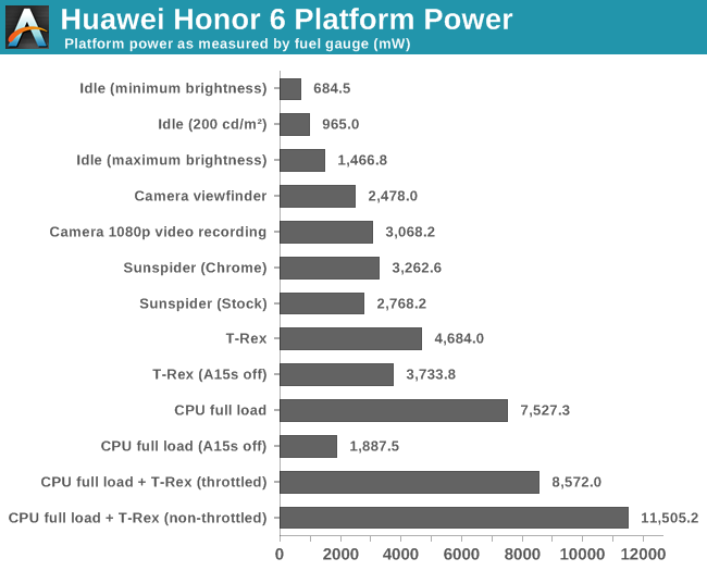
First we see that the device's idle power at our standardised 200cd/m² measuring brightness comes in at 965mW, for comparison Anand did a similar measurement for the Galaxy S5 which came in at 854mW with its AMOLED screen. Further investigating minimum brightness at 684mW and maximum brightness at 1466mW gives us about an estimated range on how efficient the JDI-manufactured panel is.
Continuing on, I tested out the camera's power usage as that is one of the most power intensive tasks for a smartphone besides playing games. At 2.5W for the preview screen and 3W for 1080p video recording we still see very reasonable values competitive with what Qualcomm and Samsung provide.
Similarly a run of Sunspider averages out at around 3W. Interesting to see here was the discrepancy between Chrome and the stock provided browser. In all test cases I was able to achieve a lower power usage on the stock browser than on Chrome. This may very well have to do with optimized CPU & GPU libraries that OEMs ship with the phone versus the more generic ones that Google bundles with Chrome.
GFXBench is when things start to get ugly: a T-Rex onscreen run averages out at 4.6W power consumption which is beyond what we find in any other competing smartphones. This really peaked my interest and tried to isolate where the power was comping from. I forcefully turned off the A15 cluster and was able to shave off almost a full 1W off the power consumption while losing only 8% of performance in the benchmark. What's left is some minor power consumption on the A7 cluster and a large chunk going to GPU and memory. When normalizing for power and peformance, the Mali T628MP4 in the Kirin 920 comes around only half the perf/W of the Adreno 330 found in the Snapdragon 801 and performs very poorly.
ARM has promised a 400% energy efficiency improvement over the T604 in the T760 and we can see why that's desperately needed, the current generation of Midgard GPUs can't compete in either performance or in power efficiency. For avid gamers, it's certainly better to look at a Qualcomm device for lack of other options in current Android devices.
While the T-Rex numbers were bad, the CPU full load ones are a disaster. Turning on a 4-thread stress test which fully loads the A15 cluster makes the device consume a whopping 7.5W. While we're going crazy might as well also try to see peak device power consumption: Running both the stress test and T-Rex in tandem results in an average power consumption of 8.5W. Here we finally see thermal throttling putting a limit to the device power as the SoC limits itself after a few seconds. Peak power comes in in at 11.5W in the intervals where the thermal mechanism clears the limits, only to re-enable them seconds later.
For academic purposes, I again disabled the A15 cluster to try to isolate power consumption on the A7 cores. The frugal nature of the Cortex A7 barely manages to exceed 1W for the cluster + memory combined.
It is clear that HiSilicon employs no power budgeting algorithms at all as the Kirin 920 leaves any kind of limiting solely to the thermal throttling driver. The problem with this approach is that you are trusting your application not to behave like a power virus. We've seen how disabling the big cluster in the T-Rex test-case can massively improve power consumption while having only little impact on performance. We have seen that is is possible to deploy a smart power allocation mechanism such as the one found in Samsung's GTS-enabled Exynos SoCs and remain within a TDP typical of a smartphone factor. This an enormous oversight in what otherwise seemed like an excellent software stack for the Kirin 920 - I hope HiSilicon in the future will resolve this issue as it's solely a software problem that's easily fixable.


59 Comments
View All Comments
semo - Friday, September 12, 2014 - link
Why no user replaceable battery? I've heard all the reasons why I shouldn't care but I still want one and wonder if planned obsolescence is the only reason for not including it.Also, is Qi an option for this phone?
Andrei Frumusanu - Friday, September 12, 2014 - link
There is no Qi charging option.semo - Friday, September 12, 2014 - link
Thanks Andrei. I think it is worthwhile pointing out this missing feature in the article just like you did with the non-removable battery. It is important for some!marcokatz - Friday, September 26, 2014 - link
Well said. Also it's important to point at that this is an Apple-wannabe that no way can match up to some of the really highly rated phones out there. /Marco from http://www.consumertop.com/best-phone-guide/Excerpt - Wednesday, October 8, 2014 - link
Yeah bro, you tell em. And Andrea why U no learn Chinese man? I wanna know what that extra stuff does. I'm going to China in like, a minute, like everyone else. What, you don't care about me bro? I love you man.And does it have haptic feed-back for goodness snakes? I want them good vibes in me fingas.
What about a sit test? Most of us reading here have fat arses, do you know sit (test)? I don't know sit (test) but I wanna hear your experience with sitting, maybe try with a heavy object like a cow, yeah a bull sit test.
That'd be great keep up the good work. <3
Murloc - Saturday, September 13, 2014 - link
1. takes up space2. makes the phone structurally weaker
2. planned obsolence/forced service you have to pay a lot for are good ways to make money
Alexey291 - Saturday, September 13, 2014 - link
Takes up literally no space seeing how Samsung S4 and S5 are both smaller and thinner than HTC One (M7 and M8 respectively)Arguably the back that's able to pop off makes the phone LESS prone to breaking as it allows the force to dissipate somewhat better than in the case of a rigid structure which simply breaks.
And lastly I am going to play the world's smallest violin for the POOR POOR manufacturers trying to make a quick buck from planned obsolescence or paid-for battery replacement.
I mean I know anandtech is all about manufacturer interests but I'll care about their concerns and problems the moment they stop earning millions upon millions in profits.
Intervenator - Saturday, September 13, 2014 - link
Are you really saying that the S4 and S5 are thinner than the HTC One because of the replaceable battery? And that it takes up "literally no space"? Really?arsjum - Saturday, September 13, 2014 - link
Not because of, in spite of.Alexey291 - Saturday, September 13, 2014 - link
Thank you sir. That's precisely what I meant. Its thinner and yet it has a replaceable battery. Impossiburu /o\To me personally all that "the replaceable battery is inefficient" nonsense is just that - nonsense. Some companies are just better at making thinner phones and some try to cut corners (and costs) at every possible stage.
And yes Anandtech has historically supported nothing but the manufacturer interests. They have been walking on these eggshells for a long time and that's precisely why they never directly criticise any dubious or greedy decision made by their sponsors :) In fact they sometimes go a step further and tell consumers (like myself) that we are wrong in wanting things like replaceable batteries and microsd slots because they are so "inefficient"
/sigh