Crucial MX100 (256GB & 512GB) Review
by Kristian Vättö on June 2, 2014 3:00 PM EST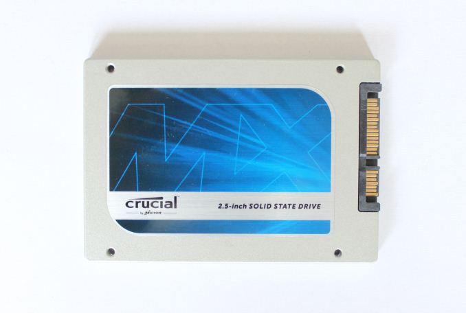
Computex is officially kicking off today and unlike many of the products announced at trade shows, we actually have a full review of the Crucial MX100 that is launching today at Computex. The MX100 is Crucial's new mainstream drive, replacing the popular M500 while the M550 will continue to serve the higher performance market. With the MX100 Crucial is aiming even lower in terms of price per gigabyte by utilizing Micron's (i.e. Crucial's parent company's) state-of-the-art 16nm 128Gbit MLC NAND. In fact the MX100 is the first mainstream product to use 16nm NAND and it's the smallest process node we have seen since Toshiba's/SanDisk's introduction of their A19nm NAND.
As we have discussed before, decreasing the lithography is the most effective way for NAND manufacturers to cut costs. The smaller lithography translates into smaller transistor size, which in turn means that the same amount of storage can be fit into a die that is physically smaller -- or you can fit more storage while keeping the die size the same. The smaller the die size, the more dies are received from each wafer, which reduces the production costs because you are basically getting more dies from the wafer without added cost. Well, almost.
For the past couple of years, every new lithography has reduced the profits and benefits that the die shrink brings. Sure the manufacturers still get more dies per wafer, but the investments required to research and manufacture the NAND have increased hand in hand with the die shrinks, making every die shrink less profitable than the previous. Furthermore, every die shrink introduces more endurance and reliability concerns because as you scale the cell, it becomes harder and harder to hold the electrons in the floating gate. That's why all major NAND manufacturers are researching 3D NAND as it will put an end (at least temporarily) to the scaling game since density can be increased by adding layers. I'll talk a bit more about the state of the NAND market and 3D NAND on the next page.
The MX100
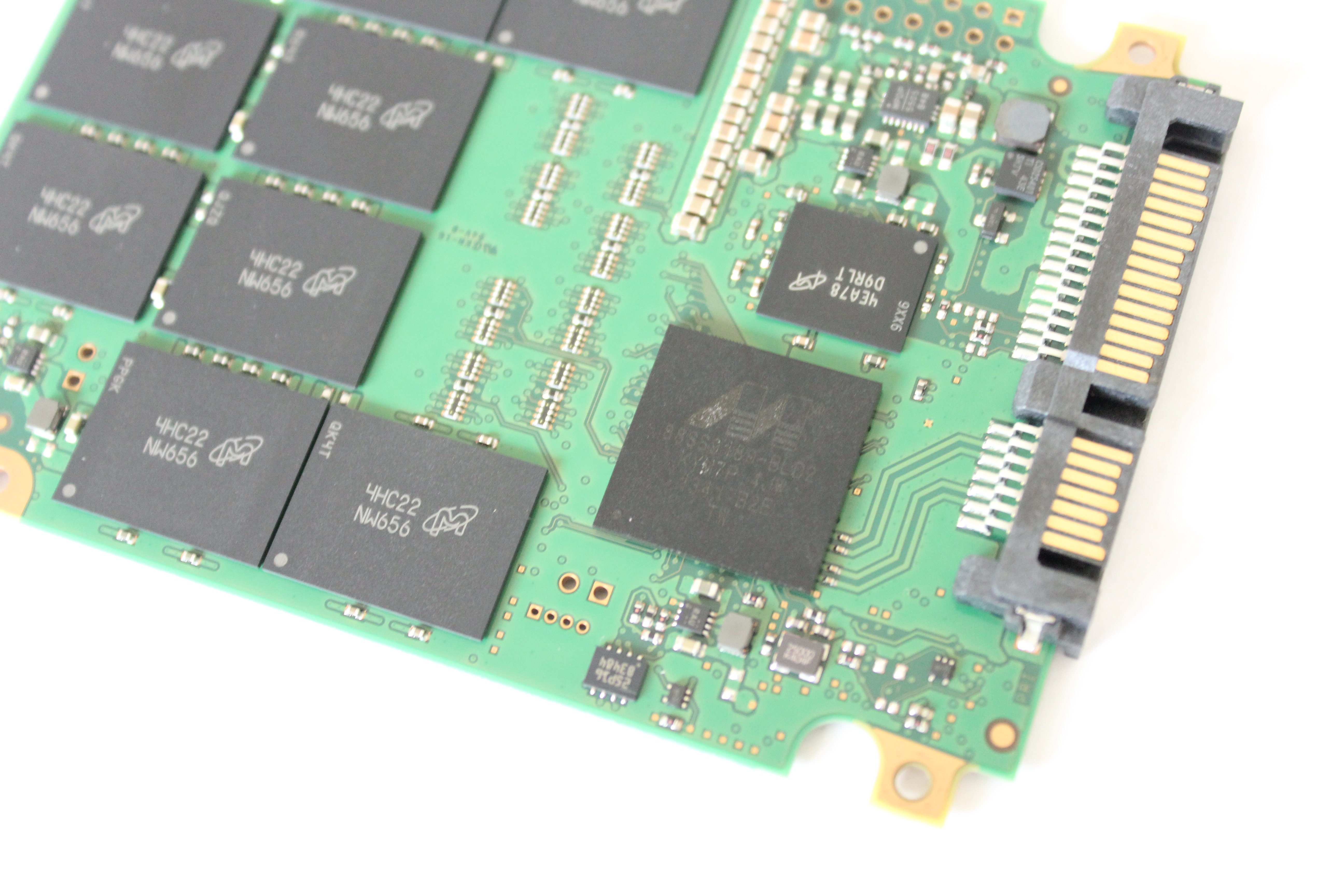
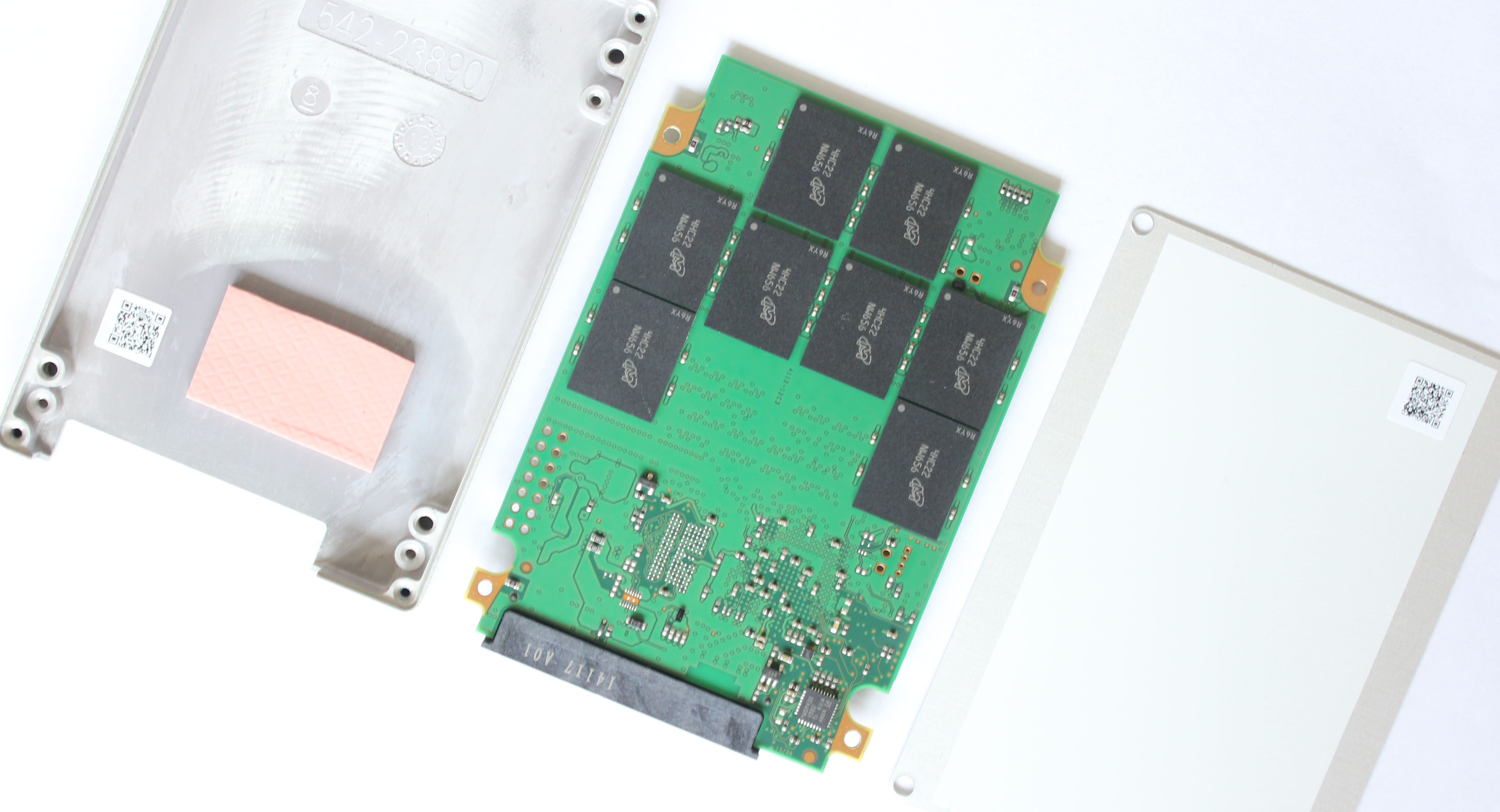
The short summary is that the MX100 builds on the same architecture as the M500 and M550. The only fundamental difference is the NAND inside as the controller is the same Marvell 88SS9189 silicon as found inside the M550. The 9189 is a minor upgrade over the 9187 and what it does is provide better support for DevSLP along with some bandwidth optimizations.
The design of the chassis and PCB remain unchanged as well, although the naming changes from Mxxx to MXxxx. I'm guessing Crucial had to change the naming because M600 would have been confusing given that the M550 will remain in the market as Crucial's high-end drive. Other than performance, Crucial is bringing some differentiation by offering limited capacities as the MX100 will only be available at up to 512GB, so those who want a larger drive will now have to pay for the M550.
| Crucial MX100 Specifications | |||
| Capacity | 128GB | 256GB | 512GB |
| Controller | Marvell 88SS9189 | ||
| NAND | Micron 16nm 128Gbit MLC | ||
| DRAM | |||
| Sequential Read | 550MB/s | 550MB/s | 550MB/s |
| Sequential Write | 150MB/s | 330MB/s | 500MB/s |
| 4KB Random Read | 80K IOPS | 85K IOPS | 90K IOPS |
| 4KB Random Write | 40K IOPS | 70K IOPS | 85K IOPS |
| Endurance | 72TB (~65GB/day for 3 years) | ||
| Encryption | AES 256-bit, TCG Opal 2.0 & IEEE-1667 | ||
| Warranty | Three years | ||
Due to the use of 128Gbit NAND, the write performance at smaller capacities takes a hit. I covered the reasons behind this in detail in the M550 review but in short the higher capacity per die means that fewer die are needed to achieve a certain capacity. This in turn reduces parallelism, which is the key of SSD performance in the first place. A single NAND die isn't very fast, but when you have multiple dies working in parallel, the performance adds up and you get hundreds of megabytes of throughput.
Feature wise the MX100 matches the M500 and M550. Both power loss protection and hardware encryption (including TCG Opal 2.0 and IEEE-1667 standards) are supported and the endurance rating remains at the same 72TB despite the change in NAND. Micron wouldn't give us the exact P/E cycle rating for their 16nm NAND but I was told that the endurance is similar to their 20nm MLC NAND. Even if there is a slight reduction in raw NAND endurance, it's possible to compensate for that by reducing the write amplification through firmware optimizations. RAIN (Redundant Array of Independent NAND) is also included to protect against page/block level failures and the parity ratio remains at 127:1 similar to the M550 (i.e. one bit of parity is generated for every 127 bits of user data).


50 Comments
View All Comments
extide - Monday, June 2, 2014 - link
Wow, 256Gbit dies! That would mean up to 2TB in a standard 2.5" SSD -- Crazy!hojnikb - Monday, June 2, 2014 - link
Actually one could fit 4TB into a standard 2.5" (or even 8GB when using 32 packages) but the problem is, as far as i can tell, no single controller can adress so much space.hojnikb - Monday, June 2, 2014 - link
*TB obviously :)extide - Monday, June 2, 2014 - link
Yeah but it's a chicken and egg thing I think. There seems to be a max price cap of about $600 for these SSD's, and so for 64gbit NAND that was ~512GB and 128Gbit NAND it is about 1TB. When they design a controller to exist during the lifetime of 256Gbit NAND there is a good chance that someone is actually going to make a 2TB drive because that much NAND would then fit inside that 'max price' so they will design the controller for that max amount. And in the same vein a contrller for the 128Gbit era would be 'OK' with a 1TB max.... if that makes sense, heh.hojnikb - Monday, June 2, 2014 - link
Also, there is already 2TBs drives out thre on the old 64Gbit flash :)danwat1234 - Monday, January 26, 2015 - link
Intel S3500 2TB exists, not sure if it works in laptops thoughfruitcrash - Wednesday, June 4, 2014 - link
It's not that you can't address it (for ONFI NAND you can use the Volume Select command), but that you can't have more than about 8 chips on a channel because of capacitive loading.extide - Monday, June 2, 2014 - link
NOTE: I am talking about the future NAND, NOT what is used in this drive.hojnikb - Monday, June 2, 2014 - link
Still, 256Gbit dies can can't help you much, if controller can't adress that much space. As i've said above, once could fit 4-8TB of flash, it's just isn't possible yet.hojnikb - Monday, June 2, 2014 - link
Any details on the 128GB version ?I've read somewhere, that it will be using the old 20nm flash...