ASUS P4T i850 Pentium 4 ATX Motherboard
by Mike Andrawes on May 9, 2001 2:56 PM EST- Posted in
- Motherboards
Baked Fresh, a Unique Design
In the past, when processors ran at relatively low FSB speeds, in the 66 to 100MHz range, signaling was not a serious issue. So most of our focus regarding the layout of a board was on the placements of components and how that affected airflow and usability..
However, that all started to change with the advent of the 133MHz FSB speed, not to mention the recent AMD EV6 bus, DDR and Rambus technology. With these new technologies having a much higher data rate, signaling has become a much more important issue for a motherboard designer. Length of traces, coupling between traces and components, noise, etc. all come into play and affect the stability of the systems. We have seen quite a few examples of the limitations of these designs, such as the Intel i815E chipset not being able to run more than four banks of memory at 133MHz, the Intel i820 chipset not reliably supporting more than 2 RIMM slots, and the majority of DDR motherboards only having two DDR DIMM slots (although with the proper design it is possible to have up to 4 DDR DIMM slots).
Proper signaling is best achieved by careful layout of the PCB. From our experience, ASUS has always put a lot of effort into truly understanding the chipset and constructing their own unique layout of the boards rather than just going with a variation on the reference design provided by the chipset manufacturer. One good example is the A7V and A7V133, which have a vertically mounted PCB with the voltage regulator. Even our recently reviewed CUV266 has a very different layout from anything else we have seen.
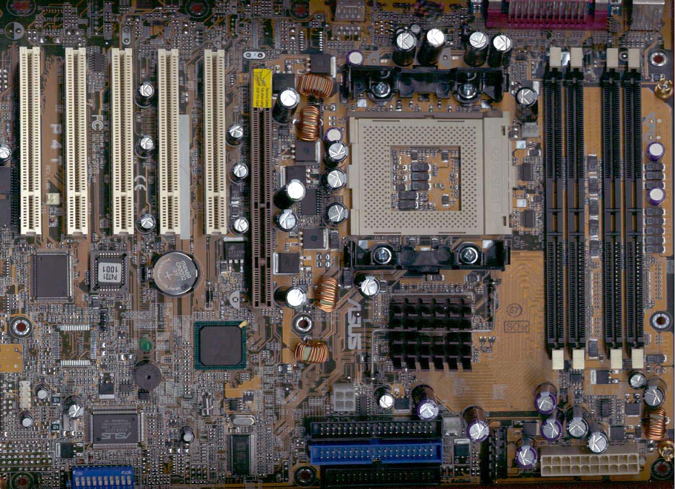
With the P4T, ASUS once again shows us that they took quite a bit of effort in redesigning the board, since the layout of the board is very different from the reference design. For starters, the 82850 Memory Controller Hub (MCH) is located close to the front of the board with the CPU socket is behind the MCH.
The most interesting part of the design lies in the RIMM slots, which are mounted parallel to the right side of the board, much like the DIMM slots of the CUV266. This design results in shorter traces, resulting in superior performance and stability.
ASUS even changed the arrangement of the RIMM slots to help boosting performance. Remember that the i850 chipset requires you ato install RIMMs in pairs, meaning that if you want to have 128MB memory you will need two 64MB RIMMs (which is exactly what Intel bundles with retail Pentium 4s). In most Pentium 4 boards, even Intel’s own reference design, the two RIMMs are installed together, and the other slots are filled with Continuity RIMM (CRIMM). However, with the P4T, you actually alternate the RIMM and the CRIMM modules. Fortunately, this is clearly documented in the manual.
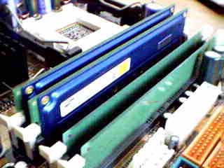
The RIMM configuration used in majority of Pentium 4 boards.
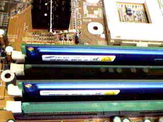
The RIMM configuration used on the P4T.
The main power supply connector is nicely placed at the front right corner, which would be relatively close to the power supply, while also preventing you from running the power cable over the CPU or memory. An “AUX” power supply connector, similar to those used on old AT form factor boards, is located beside the regular power supply connector.
The IDE and floppy controllers are located in front of the 82850 MCH so they will not block any of the expansion slots. Since the RIMM slots are now placed along the right side of the board, you don’t have to worry about not being able to install memory after installing the video card, a minor problem we see all too often.


0 Comments
View All Comments