VIA's KT133A - Overclocking w/ the 133MHz FSB: The "Issue"
by Mike Andrawes on March 20, 2001 2:09 AM EST- Posted in
- Guides
Digging Deeper
The following diagram illustrates all the combinations of the L6 bridges and their corresponding multiplier values. With the help from DaddyG of the AnandTech Forums we see how the bridges set the multiplier.
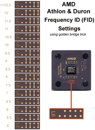
Basically when you look at the L6 Bridge, starting from the end with the extra one dot, the four pairs of bridges correspond to multiplier adder values of 1/2, 1, 2, and 4, which of course is just binary (2^-1=1/2, 2^0=1, 2^1=2, and 2^2=4). Add all the values correspond to open bridges. Then, if the value is between 0 and 1.5, add 11 to obtain the clock multiplier, and if the value is between 2 and 7.5, add 3 to obtain the clock multiplier.
Let’s take our 800MHz Athlon as an example once more. The L6 bridge is shown below. The two open bridges correspond to values of 1 and 4; add them up and you get 5. Since the value is between 2 and 7.5, you add 3 and that’s how the multiplier of 8 is derived.
Since L6 corresponds to FID, and we already know that setting BP_FID below the FID results in a fully functional CPU running at a lower than default multiplier, it is possible that we could only modify the L6 bridge to lower the default multiplier.
In order to prove this theory, we used two AMD chips, one 750MHz and one 800MHz, on the a KT133A board, with the clock multiplier set at default. With the chips untouched, they booted at 750MHz and 800MHz respectively. From the above diagram you can see that the L6 bridges on both 750MHz and 800MHz chips can be modified to that of a 700MHz chip easily by connecting one bridge. When we booted up the system with these chips, both were recognized to have a multiplier of 7 and booted up at 700MHz. The rest of the story is just a matter of choosing the best bridge to modify.
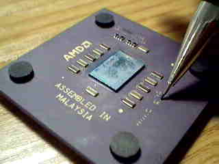
For the sake of saving time we used a pencil to actually make
the connection between the bridges. However as we outlined
in our Athlon Overclocking Guide, we strongly recommend you
use conductive ink or epoxy to make the connections.
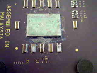
Athlon 750: Notice the pencil mark on the left most L6 Bridge to change the
multiplier from 7.5 to 7
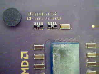
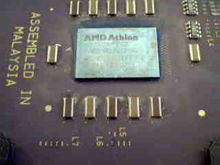
Athlon 750: The L3 and L4 Bridges are left untouched
Athlon 800: Notice the pencil mark on the second L6 Bridge from the left. Clock
multiplier changed from 8 to 7
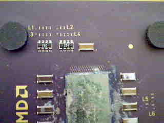
Athlon 800: Once again, the L3 and L4 Bridges are left untouched
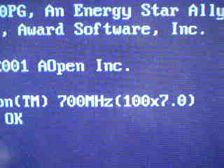
Both the modified Athlon 750 and Athlon 800 are booted at 700MHz when the multiplier
on the board is set to default.
Notice that once you past the POST, you can enter BIOS and change the clock multiplier to your desired value, provided that the L1 bridge are all closed. For example, if you intend to run your chip at 7.5 multiplier, but using the method we discussed here the multiplier is changed to 7, you can always boot up your computer at 933MHz (7x133MHz), then enter the BIOS and change the multiplier to 7.5.
If you want to help things along a bit, you can increase the default voltage the CPU will request by modifying the L7 bridges - the easiest is to just connect all L7 bridges, which indicates a voltage of 1.85V. Keep in mind that a normal Athlon has a default voltage of 1.7V and chips of 1GHz and above are set to run at 1.75V, whereas all Durons are set to run at 1.5V.
Unfortunately, certain CPUs will require you to cut a bridge to lower the multiplier, just because of the default multiplier on that particular CPU. One example is the 1.1GHz Athlon, which has a multiplier of 11, meaning that all L6 bridges are closed at the fab. In that case, you are forced to cut one bridge to bring down the clock multiplier.


0 Comments
View All Comments