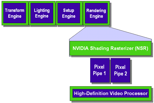
The GeForce2 MX, as the name implies, is based on the GeForce2 GTS core. The main difference being that this 0.18-micron chip only features two rendering pipelines whereas the GeForce2 GTS features a total of four. If you recall, the original GeForce even had four rendering pipelines as well. This would make you think that the GeForce2 MX would have a fill rate equal to half of that of a GeForce, but also keep in mind that one of the improvements the GeForce2 GTS offered over the original GeForce was that the GeForce2 GTS could process two textures per pipeline in a single clock whereas its predecessor could only process one texture per pipeline in a single clock.
Figure 1: GeForce2 GTS
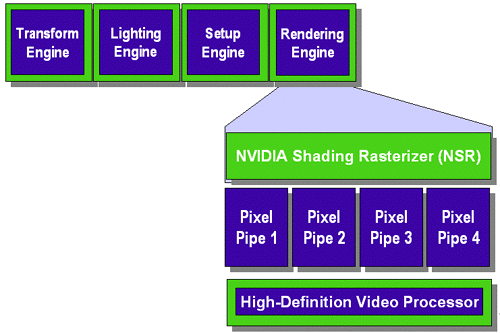
Since the GeForce2 MX is based upon the GeForce2 GTS core, its two rendering pipelines are also capable of processing two textures each in a single clock. Without discussing shipping clock speeds at all, the GeForce2 MX and the original GeForce would theoretically have the same fill rate if they were clocked at the same frequency since the GeForce had four rendering pipelines and could process one texture per pipeline (4 pipelines x 1 texture per clock = 4 texels per clock) and the GeForce2 MX has two rendering pipelines but can process two textures per pipeline (2 pipelines x 2 textures per clock = 4 textures per clock).
Figure 2: GeForce2 MX
As we learned in our review of STMicro’s KYRO based on the PowerVR Series 3 chipset, whenever a graphics accelerator has to make two passes to render a pixel it must resend all geometry data again for that second pass. So in the case of the GeForce vs the GeForce2 MX, if the number of textures for a single pixel exceeds 1 on a GeForce then the chip must resend all geometry data for each subsequent pass whereas if there are two textures being applied to a single pixel on a GeForce2 MX it doesn’t need to resend the geometry data since the texturing occurs within a single pass.
As we mentioned above the GeForce2 MX is a 0.18-micron chip, just like the GeForce2 GTS, and likewise it should be able to hit a virtually identical clock speed with the same amount of cooling. But remember that the GeForce2 MX is directed at a more cost conscious market, so instead of clocking the chip at 200MHz like its bigger brother NVIDIA chose to ditch the heatsink/fan completely from the list of requirements and clock the GeForce2 MX at 175MHz.
At 175MHz, with only two rendering pipelines the GeForce2 MX consumes half the power of the GeForce2 GTS and one-fourth the power of the GeForce 256 which results in a consumption figure of around 4W versus 8W – 9W for the GeForce2 GTS and 16W for the GeForce 256.
Now that we have the clock speed and the rendering pipelines down a bit of simple math will tell us that the GeForce2 MX has a pixel fill rate of 350 megapixels per second. This is lower than the 480 megapixels per second pixel fill rate of the original GeForce 256 and obviously lower than the 800 megapixels per second fill rate of the GeForce2 GTS. Fortunately there’s no reason to get alarmed here because the only case in which this will result in the GeForce2 MX being slower than the GeForce 256 is under single textured games which are pretty much non-existent now.
With a pixel fill rate of 350 megapixels per second and the ability to apply two textures at a time, you get a texel fill rate of 700 megatexels per second. This, being the more important number to look at, is much greater than the 480 megatexels/s fill rate of the GeForce 256 and clearly less than the 1600 megatexels/s fill rate of the GeForce2 GTS. But as we’re about to find out, something else is going to stand in the way of the GeForce2 MX before its fill rate can become a limitation.


3 Comments
View All Comments
Dr AB - Friday, May 8, 2020 - link
So 20 years laters I can say it is analogous to MAX-Q cards that we see today? Seems same logic behind it.Dr AB - Friday, May 8, 2020 - link
*laterOtritus - Friday, October 2, 2020 - link
The logic behind MAX-Q is severely reduce clock speeds and voltage to reduce power consumption. This is analogous to entry-level gpus such as tu117 in the gtx 1650. Cut down the hardware to reduce cost and power consumption, and have slightly lower clocks to hit tdp targets.