NVIDIA GeForce GTX 680 Review: Retaking The Performance Crown
by Ryan Smith on March 22, 2012 9:00 AM EST“How do you follow up on Fermi?” That’s the question we had going into NVIDIA’s press briefing for the GeForce GTX 680 and the Kepler architecture earlier this month. With Fermi NVIDIA not only captured the performance crown for gaming, but they managed to further build on their success in the professional markets with Tesla and Quadro. Though it was a very clearly a rough start for NVIDIA, Fermi ended up doing quite well in the end.
So how do you follow up on Fermi? As it turns out, you follow it up with something that is in many ways more of the same. With a focus on efficiency, NVIDIA has stripped Fermi down to the core and then built it back up again; reducing power consumption and die size alike, all while maintaining most of the aspects we’ve come to know with Fermi. The end result of which is NVIDIA’s next generation GPU architecture: Kepler.
Launching today is the GeForce GTX 680, at the heart of which is NVIDIA’s new GK104 GPU, based on their equally new Kepler architecture. As we’ll see, not only has NVIDIA retaken the performance crown with the GeForce GTX 680, but they have done so in a manner truly befitting of their drive for efficiency.
| GTX 680 | GTX 580 | GTX 560 Ti | GTX 480 | |
| Stream Processors | 1536 | 512 | 384 | 480 |
| Texture Units | 128 | 64 | 64 | 60 |
| ROPs | 32 | 48 | 32 | 48 |
| Core Clock | 1006MHz | 772MHz | 822MHz | 700MHz |
| Shader Clock | N/A | 1544MHz | 1644MHz | 1401MHz |
| Boost Clock | 1058MHz | N/A | N/A | N/A |
| Memory Clock | 6.008GHz GDDR5 | 4.008GHz GDDR5 | 4.008GHz GDDR5 | 3.696GHz GDDR5 |
| Memory Bus Width | 256-bit | 384-bit | 256-bit | 384-bit |
| Frame Buffer | 2GB | 1.5GB | 1GB | 1.5GB |
| FP64 | 1/24 FP32 | 1/8 FP32 | 1/12 FP32 | 1/12 FP32 |
| TDP | 195W | 244W | 170W | 250W |
| Transistor Count | 3.5B | 3B | 1.95B | 3B |
| Manufacturing Process | TSMC 28nm | TSMC 40nm | TSMC 40nm | TSMC 40nm |
| Launch Price | $499 | $499 | $249 | $499 |
Technically speaking Kepler’s launch today is a double launch. On the desktop we have the GTX 680, based on the GK104 GPU. Meanwhile in the mobile space we have the GT640M, which is based on the GK107 GPU. While NVIDIA is not like AMD in that they don’t announce products ahead of time, it’s a sure bet that we’ll eventually see GK107 move up to the desktop and GK104 move down to laptops in the future.
What you won’t find today however – and in a significant departure from NVIDIA’s previous launches – is Big Kepler. Since the days of the G80, NVIDIA has always produced a large 500mm2+ GPU to serve both as a flagship GPU for their consumer lines and the fundamental GPU for their Quadro and Tesla lines, and have always launched with that big GPU first. At 294mm2 GK104 is not Big Kepler, and while NVIDIA doesn’t comment on unannounced products, somewhere in the bowels of NVIDIA Big Kepler certainly lives, waiting for its day in the sun. As such this is the first NVIDIA launch where we’re not in a position to talk about the ramifications for Tesla or Quadro, or really for that matter what NVIDIA’s peak performance for this generation might be.
Anyhow, we’ll jump into the full architectural details of GK104 in a bit, but let’s quickly talk about the specs first. Unlike Fermi or AMD’s GCN, Kepler is not a brand new architecture. To be sure there are some very important changes, but at a high level the workings of Kepler have not significantly changed compared to Fermi. With Kepler what we’re ultimately looking at is a die shrunk distillation of Fermi, and in the case of GK104 that’s specifically a distillation of GF114 rather than GF110.
Starting from the top, GTX 680 features a fully enabled GK104 GPU – unlike the first generation of Fermi products there are no shenanigans with disabled units here. This means GTX 680 has 1536 CUDA cores, a massive increase from GTX 580 (512) and GTX 560 Ti (384). Note however that NVIDIA has dropped the shader clock with Kepler, opting instead to double the number of CUDA cores to achieve the same effect, so while 1536 CUDA cores is a big number it’s really only twice the number of cores of GF114 as far as performance is concerned. Joining those 1536 CUDA cores are 32 ROPs and 128 texture units; the number of ROPs is effectively unchanged from GF114, while the number of texture units has been doubled. Meanwhile on the memory and cache side of things GTX 680 features a 256-bit memory bus coupled with 512KB of L2 cache.
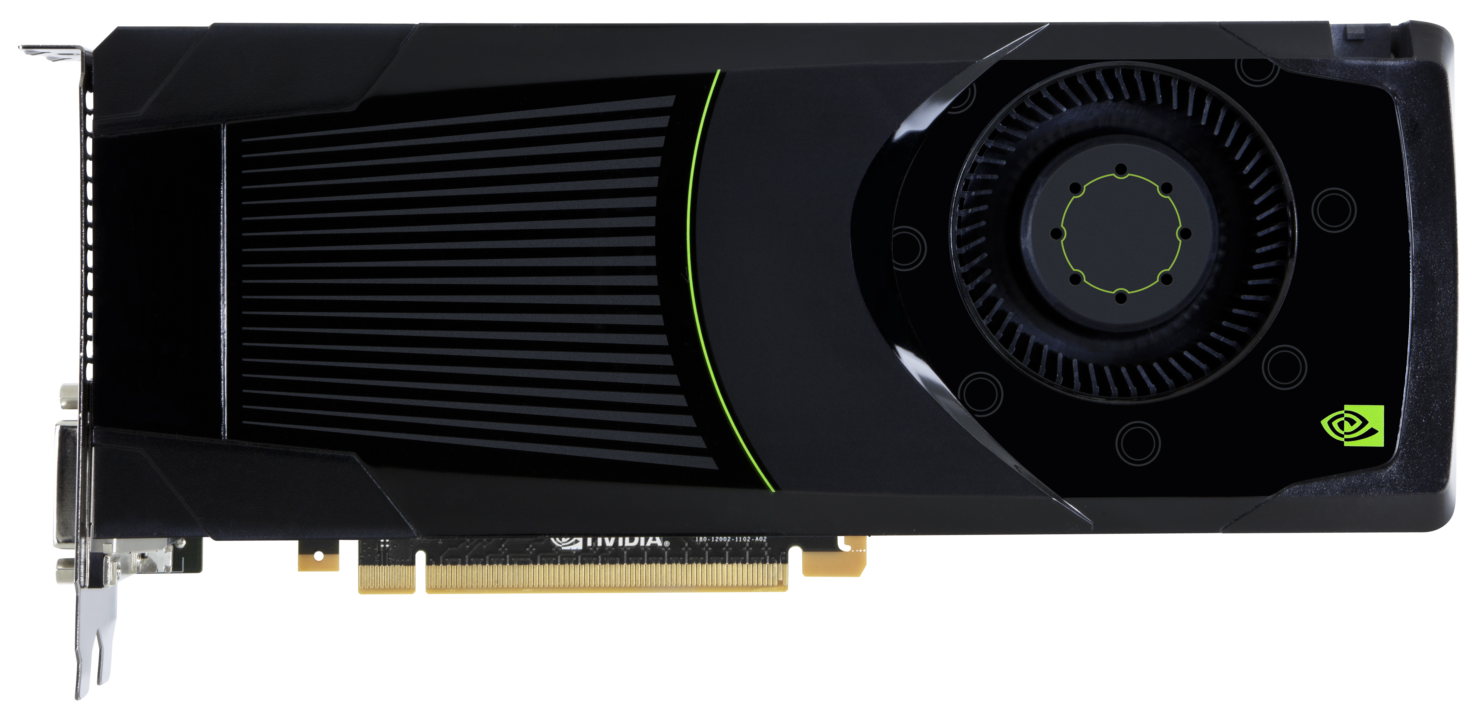
As for clockspeeds, GTX 680 will introduce a few wrinkles courtesy of Kepler. As we mentioned before, the shader clock is gone in Kepler, with everything now running off of the core clock (or as NVIDIA likes to put it, the graphics clock). At the same time Kepler introduces the Boost Clock – effectively a turbo clock for the GPU – so we still have a 3rd clock to pay attention to. With that said, GTX 680 ships at a base clock of 1006MHz and a boost clock of 1058MHz. On the memory side of things NVIDIA has finally managed to fully hammer out their memory controller, allowing NVIDIA to ship with a memory clock of 6.006GHz.
Taken altogether, on paper GTX 680 has roughly 195% the shader performance, 260% the texture performance, 87% of the ROP performance, and 100% of the memory bandwidth of GTX 580. Or as compared to its more direct ancestor the GTX 560 Ti, GTX 680 has 244% of the shader performance, 244% of the texture performance, 122% of the ROP performance, and 150% of the memory bandwidth of GTX 560 Ti. Compared to GTX 560 Ti NVIDIA has effectively doubled every aspect of their GPU except for ROP performance, which is the one area where NVIDIA believes they already have enough performance.
On the power front, GTX 680 has a few different numbers to contend with. NVIDIA’s official TDP is 195W, though as with the GTX 500 series they still consider this is an average number rather than a true maximum. The second number is the boost target, which is the highest power level that GPU Boost will turbo to; that number is 170W. Finally, while NVIDIA doesn’t publish an official idle TDP, the GTX 680 should have an idle TDP of around 15W. Overall GTX 680 is targeted at a power envelope somewhere between GTX 560 Ti and GTX 580, though it’s closer to the former than the latter.
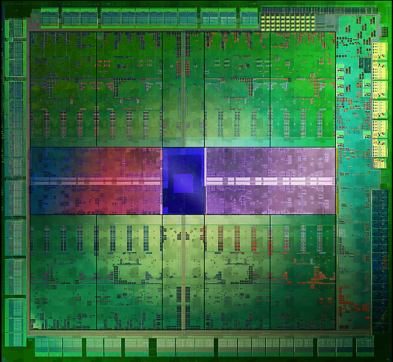
As for GK104 itself, as we’ve already mentioned GK104 is a smaller than average GPU for NVIDIA, with a die size of 294mm2. This is roughly 89% the size of GF114, or compared to GF110 a mere 56% of the size. Inside that 294mm2 NVIDIA packs 3.5B transistors thanks to TSMC’s 28nm process, only 500M more than GF110 and largely explaining why GK104 is so small compared to GF110. Or to once again make a comparison to GF114, this is 1050M (53%) more than GF114, which makes the fact that GK104 doubles most of GF114’s functional units all the more surprising. With Kepler NVIDIA is going to be heavily focusing on efficiency, and this is one such example of Kepler’s efficiency in action.
Last but not least, let’s talk about pricing and availability. GTX 680 is the successor to GTX 580 and NVIDIA will be pricing it accordingly, with an MSRP of $500. This is the same price that the GTX 580 and GTX 480 launched at back in 2010, and while it’s consistent for an x80 video card it’s effectively a conservative price given GK104’s die size. NVIDIA does need to bring their pricing in at the right point to combat AMD, but they’re in no more of a hurry than AMD to start any price wars, so it’s conservative pricing all around for the time being.
AMD’s competition of course is the recently launched Radeon HD 7970 and 7950. Priced at $550 and $450, the GTX 680 sits right in between them in terms of pricing. However with regard to gaming performance the GTX 680 is generally more than a match for the 7970, which is going to leave AMD in a tough spot. AMD’s partners do have factory overclocked cards, but those only close the performance gap at the cost of an even wider price gap. NVIDIA has priced the GTX 680 to undercut the 7970, and that’s exactly what will be happening today.
As for availability, we’re told that it should be similar to past high end video card launches, which is to say it will be touch and go. As with any launch NVIDIA has been stockpiling cards but it’s still a safe bet that GTX 680 will sell out in the first day. Beyond the initial launch it’s not clear whether NVIDIA will be able to keep up with demand over the next month or so. NVIDIA has been fairly forthcoming to their investors about how 28nm production is going, and while yields have been acceptable TSMC doesn’t have enough wafers to satisfy all of their customers at once, so NVIDIA is still getting fewer wafers than they’d like. Until very recently AMD’s partners have had a difficult time keeping the 7970 in stock, and it’s likely it will be the same story for NVIDIA’s partners.


404 Comments
View All Comments
Wreckage - Thursday, March 22, 2012 - link
Impressive. This cards beats AMD on EVERY level! Price, performance, features, power..... every level. AMD paid the price for gouging it's customers, they are going to lose a ton of marketshare. I doubt they have anything to match this for at least a year.Creig - Thursday, March 22, 2012 - link
The review has been up for less than a minute so you couldn't possibly have read it already. How pathetic is it that you were sitting there hitting F5 repeatedly just so you could get in another "First post! Nvidia is uber!" comment.Get a life.
Grooveriding - Thursday, March 22, 2012 - link
Haha Creig,Good observation, he must of been sitting there spamming to get in that first comment, before he read a word of the review.
Sour grapes at being banned much, Wreckage ?
nathanddrews - Thursday, March 22, 2012 - link
... but he's correct. The 680 does dominate in nearly every situation and category."the GTX 680 is faster, cooler, and quieter than the Radeon HD 7970. NVIDIA has landed the technical trifecta, and to top it off they’ve priced it comfortably below the competition."
Obvioulsy Wreckage's analysis of AMD's "price gouging" and prophesies of doom are farfetched...
N4g4rok - Thursday, March 22, 2012 - link
Well, yeah, the card does well in most of those tests, but i think it might be a little too far to say that it dominates the 7970 on every level.cactusdog - Thursday, March 22, 2012 - link
Just finsished looking around various sites and the 680 isnt as good as was suggested.Dont forget, you're basically comparing an overclocked Nvidia card to a stock AMD card, and even the base clock is much higher on the nvidia card.
At the same clocks the results will look much better for AMD. Also, 3 monitor gaming could favour AMD with 3GB of vram.
Seems like Nvidia really wanted to target the 7970 and the price/performance tag this time, by building a souped up, overclocked Gk104 but its not a 7970 killer. AMD will just need to sell them for $449.
AMD can stay with the 7970 as planned until Q4 and the 8 series.
gamerk2 - Thursday, March 22, 2012 - link
You know clocks aren't the only thing that determines speed? Couldn't one just as easily argue that AMD cards were better because they basically clocked their RAM so high?Fact is, at stock, the card beats the 7970 at a lower price. Period.
Meaker10 - Thursday, March 22, 2012 - link
You're ignoring the host of factory overclocked models out there that will be quieter than the 680M and perform on a similar level, the price just needs to be dropped.Kakkoii - Thursday, March 22, 2012 - link
Herp derp, the same can be said about Nvidia cards as well. The 680 has tonnes of OC'ing headroom. The GPU boost it has is a messily overclock.CeriseCogburn - Thursday, March 22, 2012 - link
I guess the lower clocked cores of 470, 480, 570, 580 , and many other Nvidia cards were greatly cheated in all benchmarks because the amd cores were often well over 100mhz higher at stock....So we have had at least 3 years of lying benchmarks in amd's favor.
I'd like to personally thank gamerk2 for this very astute observation that sheds the light of Nvidia asbolutely winning in all the above mentioned nvidia cars for the past couple of years.
Thank you... (sarc/reality check is free)