Intel's 820 Chipset - Performance using SDRAM
by Anand Lal Shimpi on January 31, 2000 4:27 AM EST- Posted in
- CPUs
The Memory Translator Hub (MTH) is an optional fourth component in the i820 chipset, the three required ones being the Memory Controller Hub (MCH), I/O Controller Hub (ICH) and Firmware Hub (FWH).
The 82805AA MTH is actually an option on both i820 and i840 motherboards, and its purpose is identical regardless of what chipset it is paired with. In order to keep things simple, we will only discuss the implementation of an MTH on an i820 motherboard.
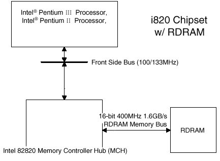
The data bus present between the i820’s MCH and the CPU is a 64-bit wide bus running at your FSB speed, which is at least 100MHz on an i820 motherboard. The job of the MCH is to handle the memory transactions that occur between the RDRAM that would normally be present on an i820 board and the CPU. On one side of the MCH, we have the 64-bit data bus that we normally refer to as the Front Side bus, and on the other side of the MCH we have the 16-bit memory bus that provides for the interface to the RDRAM slots on your motherboard. Keep in mind that this 16-bit memory bus can be running at speeds of up to 400MHz while transferring on both the rising and falling edges of the clock. Let’s take a step back and analyze exactly what’s going on here before we proceed to complicate things.
Let’s say that you start out at point A and just entered an 8-lane highway where the maximum speed is 60 mph (the Front Side Bus), you then pass under bridge (the MCH) where, on the other end, the road emerges as a 2-lane highway where the maximum speed is 240 mph (the RDRAM memory bus). As you can imagine, crossing this bridge would create quite a bit of a traffic jam, trying to squeeze 8 lanes of cars into an emerging 2 lane highway, but the pace should definitely pick up on the other end of the bridge.
Now that we’ve simplified the existing i820 motherboard design, let’s go ahead and complicate it a bit by adding in the Memory Translator Hub that we started to talk about. The MTH works by intercepting the RDRAM requests over the memory bus and translates them into SDRAM requests fed to up to 2 DIMM slots located on the other end of the MTH. Let’s plug this into our highway example from earlier and see how congested things get with the introduction of the MTH.
Let’s say you emerge from the bridge on a 2 lane highway where the maximum speed is 240 mph (the RDRAM memory bus) but then you’re immediately fed into another bridge (the MTH). On the other side of this bridge you have another 8-lane highway where the speed has been decreased to 60 mph yet again and you finally end up to where you were trying to get to, point B. As you can tell, going from point A to point B in this complicated system of highways and bridges isn’t the most efficient in the world, and if you take into account going back and forth from point A to point B and from point B to point A, then this system has no efficiency.
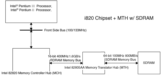
What this is all building up to is how the Memory Translator Hub actually works; it intercepts the RDRAM memory calls and translates them into SDRAM requests and then does the exact opposite before sending the data back to the MCH. What this is in explanation is preparing you for is the end result, which is a fairly significant drop in performance because of this added translation stage.


1 Comments
View All Comments
darwiniandude - Thursday, August 1, 2013 - link
Don't think I'll go i820 for my next machine, I'll stick with my current Apollo Pro 133A based mobo.