AMD's Graphics Core Next Preview: AMD's New GPU, Architected For Compute
by Ryan Smith on December 21, 2011 9:38 PM ESTAnd Many Compute Units Make A GPU
While the compute unit is the fundamental unit of computation, it is not a GPU on its own. As with SIMDs in Cayman it’s a configurable building block for making a larger GPU, with a GPU implementing a suitable number of CUs in multiples of 4. Like past GPUs this will be the primary way to scale the GPU to the desired die size, but of course this isn’t the only element of the design that scales.
With a suitable number of CUs in hand, it’s time to attach the rest of units that make up a GPU. As this is a high-level overview on the part of AMD they haven’t gone into great deal on what each unit does and how it does it, but as the first GCN product gets closer to launching the picture will take on a more complete form.
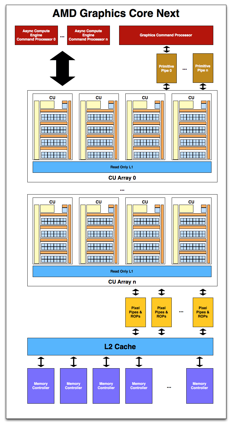
Starting with memory and cache, GCN will once more pair its L2 cache with its memory controllers. The architecture supports 64KB or 128KB of L2 cache per memory controller, and given that AMD’s memory controllers are typically 64bits each, this means a Cayman-like design would likely have 512KB of L2 cache. The L2 cache is write-back, and will be fully coherent so that all CUs will see the same data, saving expensive trips to VRAM for synchronization. CPU/GPU synchronization will also be handled at the L2 cache level, where it will be important to maintain coherency between the two in order to efficiently split up a task between the CPU and GPU. For APUs there is a dedicated high-speed bus between the two, while discrete GPUs will rely on PCIe’s coherency protocols to keep the CPU and dGPU in sync.
Meanwhile on the compute side, AMD’s new Asynchronous Compute Engines serve as the command processors for compute operations on GCN. The principal purpose of ACEs will be to accept work and to dispatch it off to the CUs for processing. As GCN is designed to concurrently work on several tasks, there can be multiple ACEs on a GPU, with the ACEs deciding on resource allocation, context switching, and task priority. AMD has not established an immediate relationship between ACEs and the number of tasks that can be worked on concurrently, so we’re not sure whether there’s a fixed 1:X relationship or whether it’s simply more efficient for the purposes of working on many tasks in parallel to have more ACEs.
One effect of having the ACEs is that GCN has a limited ability to execute tasks out of order. As we mentioned previously GCN is an in-order architecture, and the instruction stream on a wavefront cannot be reodered. However the ACEs can prioritize and reprioritize tasks, allowing tasks to be completed in a different order than they’re received. This allows GCN to free up the resources those tasks were using as early as possible rather than having the task consuming resources for an extended period of time in a nearly-finished state. This is not significantly different from how modern in-order CPUs (Atom, ARM A8, etc) handle multi-tasking.
On the other side of the coin we have the graphics hardware. As with Cayman a graphics command processor sits at the top of the stack and is responsible for farming out work to the various components of the graphics subsystem. Below that Cayman’s dual graphics engines have been replaced with multiple primitive pipelines, which will serve the same general purpose of geometry and fixed-function processing. Primative pipelines will be responsible for tessellation, geometry, and high-order surface processing among other things. Whereas Cayman was limited to 2 such units, GCN will be fully scalable, so AMD will be able to handle incredibly large amounts of geometry if necessary.
After a trip through the CUs, graphics work then hits the pixel pipelines, which are home to the ROPs. As it’s customary to have a number of ROPs, there will be a scalable number of pixel pipelines in GCN; we expect this will be closely coupled with the number of memory controllers to maintain the tight ROP/L2/Memory integration that’s so critical for high ROP performance.
Unfortunately, those of you expecting any additional graphics information will have to sit tight for the time being. As was the case with NVIDIA’s early reveal of Fermi in 2009, AFDS is a development show, and GCN’s early reveal is about the compute capabilities rather than the graphics capabilities. AMD needs to prime developers for GCN now, so that when GCN appears in an APU developers are ready for it. We’ll find out more about the capabilities of the ROPs, the primitive pipelines, the texture mapping units, the display controllers and other dedicated hardware blocks farther down the line.
In the meantime AMD did throw out one graphics tidbit: partially resident textures (PRT). PRTs allow for only part of a texture to actually be loaded in memory, allowing developers to use large textures without taking the performance hit of loading the entire texture into memory if parts of it are going unused. John Carmack already does something very similar in software with his MegaTexture technology, which is used in the id Tech 4 and id Tech 5 engines. This is essentially a hardware implementation of that technology.


83 Comments
View All Comments
StormyParis - Friday, June 17, 2011 - link
Thank you for a very enlightening write up. Comments and questions:1- please add a comma in there somewhere. I had to read the sentence 4 times to understand it (page 1=: "VLIW designs will never achieve perfect efficiency in this regard, but the farther off real world utilization is the weaker the benefits of VLIW."
2- When, if ever, will we vile users see any benefits ? I get the feeling that most apps are still not optimized well, if at all, for multicore/threading. Come to think of it, most don't even use most of the x86 extensions more recent than SSE2. Now we're talking of yet another x86 extension, that is not only AMD-specific, but very task-specific. Apart from a handful of labs doing GPU computing, and the usual Photoshop filters... i'm doubtful ?
MonkeyPaw - Friday, June 17, 2011 - link
I'm not an expert in this sort of design, but is AMD setting up this architecture to replace the x86 ALU? Bulldozer is already running 2 ALUs for every 1 FPU, which is promoting ALU-heavy software design. It may take a few revisions to meld them (or phase one out), but it certainly seems like that's a heterogeneous CPU in the end.marc1000 - Friday, June 17, 2011 - link
there is a slide (on Llano article, I believe) where AMD points this. yes, they want to completely merge them, and the ALU would be one of this mergind points.A5 - Friday, June 17, 2011 - link
I think it'll be quite awhile before the monolithic cores dissolve into the heterogeneous architectures, mostly depending on how fine-grained the power gating can get. When it gets to the point where the CPU can selectively turn off components inside a given SIMD unit, I think we'll see someone go "Wait a minute, then why do we even have this big core anymore?" and it'll go away. 2018ish, maybe?jamescox - Monday, June 20, 2011 - link
ALU is generally used to refer to a very simple unit that performs arithmetic, logic, and possibly bit shift operations on integers, not floating point values. The units labeled ALU in the GPU diagrams in the article may support some integer operations, but they mainly process 32-bit floating point values, and (IMO) should not be labeled as "ALUs". FPU would probably be more accurate, but I do not know what operations these units support and whether they include a native integer ALU or just convert to integers to FP.
I don't know what you would mean by ALU-heavy software design. Bulldozer has two integer execution cores per module. Each core is composed of 2 ALUs and 2 AGUs, not shared. It also has 2 128-bit floating point (FMA) units per module shared between the two threads. This isn't really much different than an intel hyper-threaded core. Intel has, I believe, 3 ALUs, 3 AGUs, and 2 FPUs per core which is shared between 2 threads. AMDs version of multi-threading just doesn't share as much hardware between threads, which may be better than Intel's HT (2-2-1 AMD vs 1.5-1.5-1 Intel ALU-AGU-FPU). Intel's version would allow a single thread to us all of the execution resources at once, if there is no competing thread. Sharing the FPU makes a lot of sense, since most code that runs on CPUs only uses the FPU intermittently. If the code uses FP more than intermittently, then it would be a candidate for vectorization, and execution on the GPU instead.
While AMDs next generation graphics hardware may be able to execute more general code compiled from a wider range of languages, it is not an x86 processor, and it can not replace the CPU. If you look at the diagram, it has a single scalar unit to handle non-vector code in each compute unit. It also has 64 units in the 4 vector arrays of each CU. If you actually tried to compile and run the kind of branch heavy, integer code that CPUs have to deal with on a CU, then it would probably run entirely and very, very slowly on that single scalar unit.
MrSpadge - Wednesday, June 22, 2011 - link
I think you've got the right idea with this being melted into a Bulldozer-like design. however, it wouldn't replace the x86 ALUs, which are highly-optimized for high clock speed and low latency execution, as well as excellent handling of branches etc.No, it would rather replace or supplement a fat FPU shared between many "cores" (which, by then would basically mean ALUs + scheduling). Most tasks which requires massive fp number crunching can be executed well in parallel and therefore are suitable for execution on a GPU core. The question is just how to bond them together so that the software guys can actually use them..
MrS
Deleted - Thursday, December 22, 2011 - link
Basically, what we have here is a math coprocessor. Back in the day, Intel's x86 processors were very good (relatively speaking) at integer math, but choked on floating point math. So Intel created the 8087 to handle the floating point calculations while the CPU handled the integer calculations (obviously this wasn't exclusive to Intel, but I'm generalizing). Eventually, the floating point unit was merged onto the CPU, and programs began using them interchangeably.What we have today is very similar. CPUs, even with their advanced FPUs, are nowhere near as powerful as the massively parallel monstrosities we use for graphics. Eventually, they will be merged onto the CPU, and used as readily for general floating point processing tasks as FPUs are currently.
And this is the point of Fusion: to fully replace the aging floating point unit with an IGP.
A5 - Friday, June 17, 2011 - link
The benefits to home or enthusiast users of heterogeneous CPUs are still several years off. We need market penetration of hardware along with fundamental changes in software development models and smarter compilers.nedwards - Tuesday, January 28, 2014 - link
Smarter programmers would help! Let me rephrase that. Programmers thinking in a parallel mindset would help!Beenthere - Friday, June 17, 2011 - link
If AMD delivers in a timely manner they will have a bright future. This looks like a huge technological transition and I understand the need to get developers onboard now but it also tips AMD's hand to Intel who will steal any ideas that they can.Unfortunately we are still waiting for most applications to be written for 64-bit use so I'm not holding out much hope for an expeditious migration on a complex technological transition though it does appear that maybe AMD has been working on this for some time and may be able to do a better job of executing with Trinity and future products. Time will tell but I hope AMD delivers on time and they will definitely get my dime - all of them.