A Closer Look at the Sandy Bridge Die
by Anand Lal Shimpi on January 10, 2011 2:29 PM EST- Posted in
- CPUs
- Intel
- Sandy Bridge
- CES 2011
Aside from a stack of Reese’s Peanut Butter Cups, I snagged something else of interest at my Intel meeting at CES 2011: a shot of some exposed Sandy Bridge processor die. As a recap SNB is available in three different physical die versions today: quad-core, dual-core with GT1 graphics and dual-core with GT2 graphics. The die sizes and transistor counts are below:
| CPU Specification Comparison | ||||||||
| CPU | Manufacturing Process | Cores | Transistor Count | Die Size | ||||
| AMD Thuban 6C | 45nm | 6 | 904M | 346mm2 | ||||
| AMD Deneb 4C | 45nm | 4 | 758M | 258mm2 | ||||
| Intel Gulftown 6C | 32nm | 6 | 1.17B | 240mm2 | ||||
| Intel Nehalem/Bloomfield 4C | 45nm | 4 | 731M | 263mm2 | ||||
| Intel Sandy Bridge 4C | 32nm | 4 | 995M | 216mm2 | ||||
| Intel Lynnfield 4C | 45nm | 4 | 774M | 296mm2 | ||||
| Intel Clarkdale 2C | 32nm | 2 | 384M | 81mm2 | ||||
| Intel Sandy Bridge 2C (GT1) | 32nm | 2 | 504M | 131mm2 | ||||
| Intel Sandy Bridge 2C (GT2) | 32nm | 2 | 624M | 149mm2 | ||||
Now for the shot:
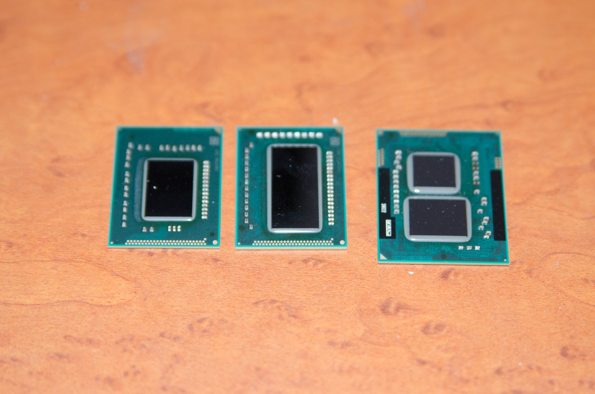
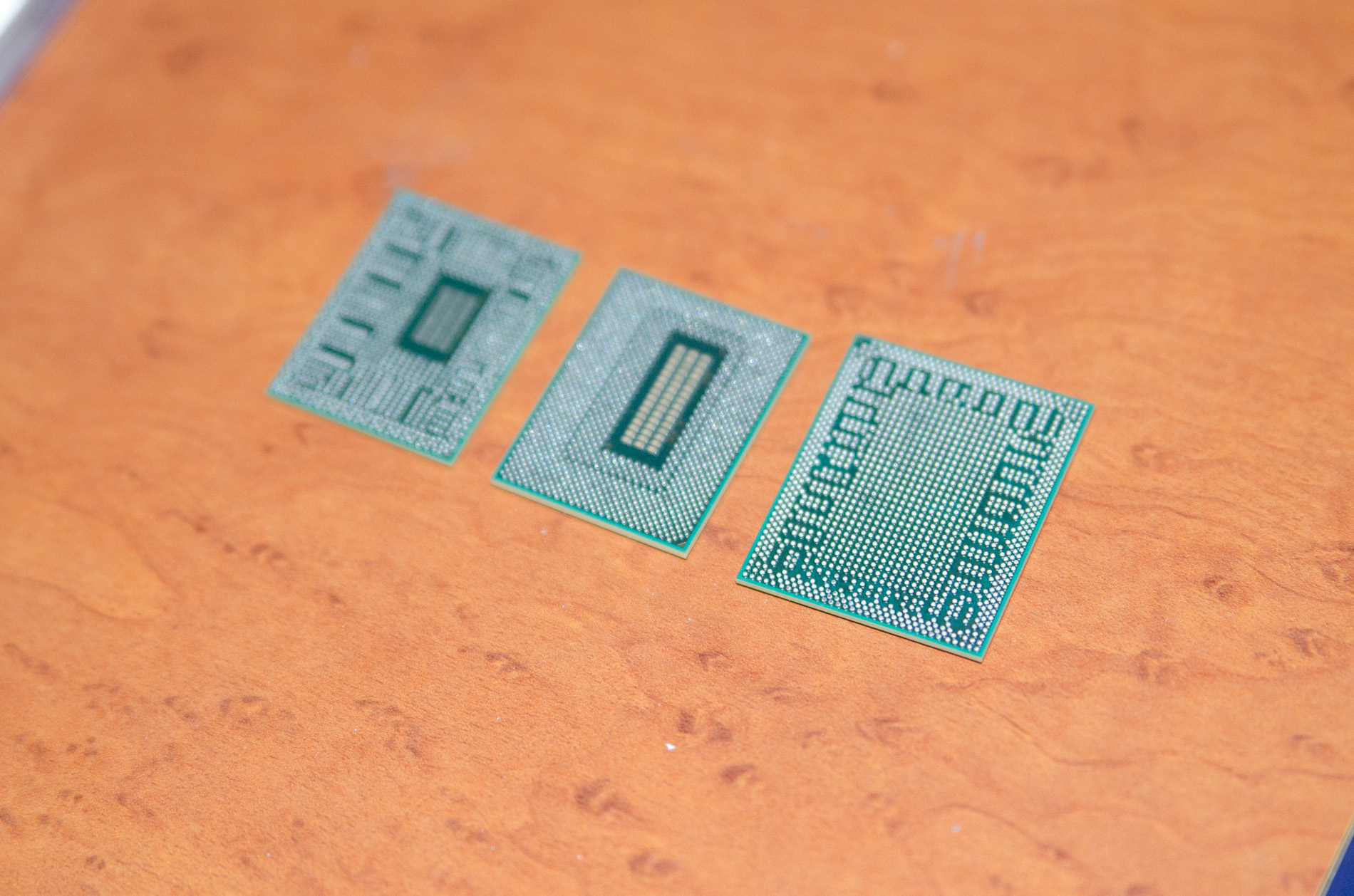
From left to right we have a dual-core GT2 die, a quad-core die and a 32nm Arrandale die with on-package 45nm HD Graphics GPU. There’s very little difference between the dual-core GT2 die and the quad-core die - each SNB core is fairly small at 32nm.
The comparison to Arrandale is also interesting as it makes dual-core SNB look pretty sensible. But keep in mind that we don’t know the full cost structure for manufacturing at 45nm vs. 32nm. Newer processes tend to be more expensive initially compared to older, more mature processes.


7 Comments
View All Comments
Stuka87 - Monday, January 10, 2011 - link
I didn't realize the form factor had shrunk from previous Core series chips.Brunnis - Monday, January 10, 2011 - link
Anand, I don't think you've mentioned what the differences between GT1 and GT2 are... Is GT2 simply 12EU while GT1 is 6EU? GT2 for mobile use while GT1 is for desktop?deputc26 - Monday, January 10, 2011 - link
It's just 12EU vs. 6EU, clocks change for mobile vs. desktop but the silicon is the same.QChronoD - Monday, January 10, 2011 - link
Maybe I missed it between all the tablets and the new 4K 3D TVs, but I haven't seen any announcements that I can remember for new Sandy Bridge laptops from CES. Are you guys going to have a roundup later?(Want something to replace a 4y/o 1.2Ghz C2D ULV... Preferably something that can play Minecraft and last 6+ hours)
iwod - Monday, January 10, 2011 - link
I remember in one of your SandyBridge Article, you mentioned Intel GPU manage to perform similar to X ATI / Nvidia GPU @ 240 Million Transistor while only using 120 Million transistor.However according to your Chart, a Single Core GT1 would actually be 120 Million transistor. And GT2 would be 240 Million.
I am also surprised Intel decided to make 2 difference die instead of having GT2 with one core cut off. 32nm must be getting very good yield in order to do so.
mczak - Monday, January 10, 2011 - link
I'm fairly confident the GT1 dual core version also only has 3MB of L3 present (some of the GT2 dual core mobile parts also have only 3MB L3 but they have 1MB disabled instead of not present).Just look at the floor plan of the quad core SB (which is the only one published), and you can pretty much see how the dual core ones will look like (and in the case of the GT1 one, why it has 1/4 less L3 cache apart from less EUs).
mczak - Monday, January 10, 2011 - link
Forgot to mention, so the 120M transistor count difference (as well as the die size difference) is only about half due to missing 6 EUs, the rest would be the 1MB L3 cache missing.Still, the overall die size difference is quite small indeed, and hardly seems worth the effort. I guess though it's because those versions will be sold in huge quantities (contrast this to LG1366 westmere, which are sold as 6-core, 4-core, 2-core, and even one-core embedded xeons, all with the one and only 6-core die, but presumably all partly-disabled parts combined in lower quantity than either of the 2 dual core SB).