VIA Apollo Pro 133A & VCSDRAM - Part 1: The Technology
by Anand Lal Shimpi on October 18, 1999 11:28 PM EST- Posted in
- CPUs
The North Bridge
 Feature-wise, the Apollo Pro 133A is
just what the doctor ordered, it combines all of the "next-generation" features
that we're looking for. Although it may not offer the same amount of memory bandwidth as
the i820, it is definitely a good solution for current 133MHz FSB CPUs, at least until
RDRAM takes off as the next standard as Intel is claiming it will become.
Feature-wise, the Apollo Pro 133A is
just what the doctor ordered, it combines all of the "next-generation" features
that we're looking for. Although it may not offer the same amount of memory bandwidth as
the i820, it is definitely a good solution for current 133MHz FSB CPUs, at least until
RDRAM takes off as the next standard as Intel is claiming it will become.
The chipset, like all of VIA's solutions, uses the familiar North/South Bridge construction with the memory, AGP and CPU interactions controlled by the North Bridge and all other peripherals (i.e. IDE controllers, PCI bus, etc…) controlled by the South Bridge. How does the new North Bridge make the Apollo Pro 133A what it is?
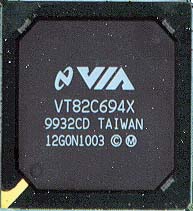
The North Bridge that makes up the chipset is the VIA VT82C694X as is seen to the right. This is the first VIA North Bridge to be manufactured out of National Semiconductor's fabrication plants, which VIA acquired earlier this year, hence the National Semiconductor logo.
The 694X is virtually identical to VIA's VT82C693A that was present as the North Bridge on Apollo Pro 133 boards. It supports the 1/2 AGP clock divider, the 133MHz FSB frequency as well as asynchronous operation of the memory bus at either the FSB frequency, FSB - 33MHz or FSB + 33MHz (combinations greater than 133MHz are not supported). This means that the memory frequencies supported by the chipset are 66MHz, 100MHz, and 133MHz. It also allows you to combine a 133MHz FSB CPU with slower PC100 SDRAM that doesn't cut it at 133MHz.
In terms of memory support, both the 694X and the older 693A support SDRAM, HSDRAM and Virtual Channel SDRAM. The read/write buffers and memory timings remain unchanged from the 693A so performance should be identical to that of the Apollo Pro 133A.
The only real difference is the addition of AGP 4X support to the chipset. This addition unfortunately increases the pin count of the 694X from 492 pins to 510 pins, making the new North Bridge incompatible with older designs. The downside to this is that it means that a motherboard manufacturer can't just 'pop' in the new North Bridge into their older 693A designs; they have to actually provide a small amount of redesigning. Fortunately the cost of adjusting a 693A design to the new 694X North Bridge is not that great, but it is a reason why you haven't seen many motherboards based on the 694X. At this year's Fall Comdex in Las Vegas we'll definitely see a number of Slot-1 and Socket-370 solutions built on the new 694X, the support for the platform is definitely there.
The CPU support that the 694X brings to the table is identical to what the BX, i820, and the older 693A offer. The chipset supports all Slot-1 CPUs including the forthcoming Pentium III E (aka Coppermine); just make sure that the particular motherboard you're interested in supports the 1.65v core voltage of the Pentium III E and you'll be fine.
As with all other VIA North Bridges, the 694X requires VIA's own GART drivers to enable full AGP 2X/4X transfer rates. This driver is available at VIA's page and has no incompatibilities with the current crop of graphics accelerators on the market, including NVIDIA's GeForce 256. VIA has come a long way since their original AGP chipsets were released for the Socket-7/Super7 platform; they have improved on the once horrendous compatibility problems their chipsets were plagued with.


0 Comments
View All Comments