NVIDIA Introduces dual Cortex A9 based Tegra 2
by Anand Lal Shimpi on January 7, 2010 2:00 PM EST- Posted in
- Smartphones
- Mobile
Tegra Tablets Today, Smartphones Soon
The original Tegra was a 65nm chip made at TSMC, this one is 40nm also made at TSMC. The die shrink gives NVIDIA the ability to cram around 2x the transistor count into the same space.
At 260M transistors, Tegra 2 is a fairly complex chip. The total die size is approximately 49mm^2, which actually sounds big given the target market. The A9s occupy around 10% of the total die area.
The initial Tegra 2 chips will be paired with an 8.8mm BGA package for use in standard tech PCBs. Smartphone versions will be in smaller packages in order to save real estate.
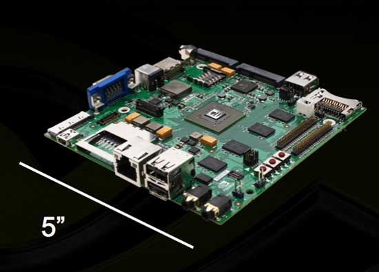
NVIDIA is supplying 5" development boards to its partners interested in Tegra 2. NVIDIA tells us that there are "hundreds" of these systems out in the wild. As you can guess by the size of the development board, the initial target for this chip isn't quite a smartphone.
The focus of today's announcement is unfortunately tablets. They are going to be able to make it to market quicker and are farther along the design process. While we don't expect any vendor to have completely nailed the perfect tablet yet, we should see some interesting UIs and form factors.
Multiple sources have now told me that the reason we never saw Tegra 1 in any smartphones or mainstream devices until the Zune HD was a simple case of NVIDIA arrogance. NVIDIA assumed that selling Tegra to phone manufacturers was just like selling GPUs to PC vendors, and it most definitely wasn't. It's been a long learning process, but NVIDIA appears to be better as a result.
There are Tegra 1 smartphones in flight right now. Presumably we'll see the first at this year's Mobile World Congress in Barcelona next month. There are also Tegra 2 smartphones that are currently being designed. We will see these before the end of 2010.


55 Comments
View All Comments
T2k - Tuesday, January 12, 2010 - link
http://www.slashgear.com/imagination-technologies-...">http://www.slashgear.com/imagination-te...gx545-to...Nvidia has nothing against Imagination's new PowerVR chip, period.
Anand is licking the wrong @ss again.
bnolsen - Monday, January 11, 2010 - link
That pat is bothersome...the core general purpose cpu being only 10% of the transistors in the package. Makes me wonder if there isn't some better way to design cpus and socs in general.techadd - Monday, January 11, 2010 - link
Most of the job is now done on specialized processors. Get used to it. The general purpose CPUs are going to matter less and less. They are slow for hard tasks and will be giving way to special gear like video and graphics processors.jconan - Saturday, January 9, 2010 - link
is the TEGRA2 CUDA compliant as others have mentioned?techadd - Sunday, January 10, 2010 - link
I doubt it. That would draw more power. It's good as it is, but I have hopes for future Tegrasjconan - Saturday, January 9, 2010 - link
is the TEGRA2 CUDA compliant as others have mentioned?Mike1111 - Saturday, January 9, 2010 - link
Anand, Imagination has their own dedicated HD video decode (VXD) and encode (VXE) processors, just like Nvidia. They offer comparable features (1080p h.264 high profile decode and encode) in a low power envelope. This has nothing to do with the GPU (SGX vs. Nvidia's 2D/3D graphics processor).VXD390: http://www.imgtec.com/news/Release/index.asp?NewsI...">http://www.imgtec.com/news/Release/index.asp?NewsI...
VXE380: http://www.imgtec.com/news/Release/index.asp?NewsI...">http://www.imgtec.com/news/Release/index.asp?NewsI...
Plus the iPhone3GS officially supports not only 480p but (720x)576p anamorphic (PAL DVD resolution) with high bitrates (if you go too high you just have to manually restrict your encoder to h.264 level 3.0 or iTunes won't transfer the file). Unofficially the iPhone 3GS supports even 1080p, you just have to know which h.264 options to tweak and how to transfer the file. So the problem with 1080p decode is Apple, not the Samsung SoC. Of course that's nothing compared to the announced Tegra2 SKU, but that's no surprise since it's newer and aimed at tablets/smartbooks etc.
thebeastie - Friday, January 8, 2010 - link
Good article this one, why? Because I had no idea Nvidia were working on a good SoC technology, I simply ignored just about ANYTHING with the word Tegra on it think it was just some power sucking first gut shot thing created by nvidia as a side show.I was so ultra wrong! This looks truly impressive.
vol7ron - Thursday, January 7, 2010 - link
Anand,You certainly hyped the A9 up, maybe a little too much. I agree with you and everything, but the repetition of the Cortex A9 support kind of made me a little sick. (please read on)
Personally, I'm happy if there are any improvements, but this still isn't where it should be. What I would like to know, though, is if you plan on doing any performance testing on phone devices in the future?
I believe smartphones/PDAs/pocket pcs - whatever you want to call them - are reaching that last step of maturity and have enough features and variance that they are worthy of testing.
I even started thinking, "should I pay to upgrade my phone?" I have 1 1/2 years left on my contract! Had this been one of my previous, non-touch devices, I would have gladly saved money and waited 'til even after my contract expired. But now, I started thinking that I'm using my phone a lot more than my desktop - the $/time-used would say it'd be a better buy.
Please start doing some in-depth analysis and, if you can, please push the phone manufacturers to include pico-projectors / good external speakers. I for one use my phone to watch my workout videos, it'd be nice just to set it down or let others view things at the same time.
vol7ron
QChronoD - Thursday, January 7, 2010 - link
Dear Santa,I plan to be very good this year, so please start your elves working on a new phone running Android on a Tegra2 with a 4.5" OLED screen.