DFI X48 LT T2R: Floats like a Butterfly…
by Rajinder Gill on April 28, 2008 4:00 AM EST- Posted in
- Motherboards
GTL - Not again!
CPU GTL reference voltage values are employed as threshold voltages by internal, on-die comparators used to determine whether each switch of an incoming data signal on either the FSB data or address busses is meant to represent a logic high or logic low (1 or 0). Adjusting these reference voltages in effect shifts the level in which the signal is seen as either high or low by the processor. As FSB is increased, the switching frequency is increased (by definition) meaning that each low to high or high to low voltage transition must occur at an accelerated rate.
This reduction in signaling margin, coupled with a more exaggerated ground bounce and overshoot, often requires manual adjustments in these thresholds if the system is to remain stable at the higher FSB speeds. Reducing or increasing the GTL reference voltages around a given percentage margin of the applied VTT by only a few millivolts can drastically affect processor stability. Imagine the processor detecting a 1 on a data transfer line when an incoming signal is in fact supposed to be low (0) - not surprising, the result is a BSOD, a complete system hang, or possibly even an undetected corruption of critical system data.
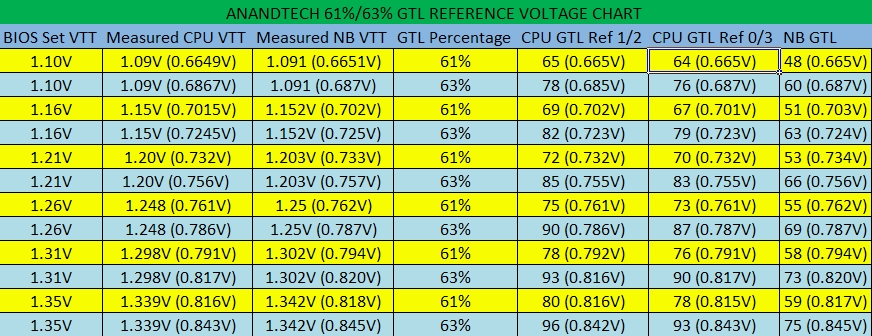
The added load capacitance of dual die processors (current Intel quad-core processors) usually requires more signaling drive as the FSB frequency is increased resulting in a need to raise VTT voltage. Any adjustment to VTT may also in turn require changes to GTL reference voltages in order to support proper data transfer margins. For 65nm processors the ratio of any GTL voltage to VTT is around 67% for both CPU and Northbridge (NB) GTL voltages; 45nm processors require that this percentage be closer to 61%-63%, again for both CPU and the NB. For example, for a VTT of 1.10V a 45nm processor would require a GTL reference voltage in the region of about 0.671V (61% of VTT) to 0.693V (63% of VTT).
DFI's approach to providing the user with ultra fine control of GTL reference voltages is unsurpassed in the motherboard industry, although working with an ultra fine scale such as this requires a significant dedication of time in order to get things right. In fact, some users enjoy this type of tweaking while others may feel it is akin to pulling teeth. In order to address this situation DFI has gone to the trouble of releasing a scale showing equivalent VTT/GTL percentages and associated BIOS settings.
We have found the scales themselves to be quite broad in range so we are providing a condensed version, taken from measurements using our own board here in the lab. The major issue here is that no two boards/CPUs are likely to behave in the exact same manner. This being the case, the small chart below is only intended to provide a starting point for any adjustments that may need to be made to your particular setup.
 |
Easy
500FSB E8500 Setup guide (easy starting point)
In order to make things as easy and presentable as possible we decided to provide users with a video setup guide showing how to run 500FSB with an Intel E8500 processor. We cannot guarantee the settings shown in the video will work on all systems as component choices will play a huge part in how far the board can clock. Secondly, GTL values vary from board to board and across processors adding further variables in to the mix. We attempted to keep the setup as simple as possible whilst enabling all key chipset registers for performance. If there is enough demand, we may venture into a quad-core overclocking guide too - although 400-420FSB is attainable with a minimum of BIOS level adjustments, so a guide is not really necessary.


24 Comments
View All Comments
orangeblue - Friday, June 13, 2008 - link
hi,can anybody tell me if the ocz flex 9200 4gb-kit(2x2048) workz too instead the four 1024 plz.
Zoomer - Saturday, May 3, 2008 - link
I miss the analysis of other features than just plain memory latency.Max fsb overclock, max mem overclock, etc?
Running the board at 400fsb seems boring - lots of P965 boards can best that. Tons of people don't buy these multiplier unlocked chips.
Rajinder Gill - Sunday, May 4, 2008 - link
Hi,Dual core 45nm's top out at around 510-515FSB using air cooling. Most of the quad CPU info is in the review.
We are looking at perhaps adding some more content tomorrow. Mainly 2x2GB and 4X1GB maxmimum stable overclocks and best operating points - using air cooling.
When Using 45nm dual core CPU's X48/X38 chipsets are really only 'good' to around 500FSB tops for 24/7, after this VMCH requirements and total stability with low tRD becomes futile rather quickly. SOme of the DDR3 boards are a little better in this regard, though this overhaed always comes at a high voltage price when used with a suitably high CPU multiplier.
65nm CPU's in dual core form may cruise upto 550fsb with some work, perhaps a 67% GTL table will help for that. Many of the benches in the review were run at 8x500FSB just to reflect the maximum 24/7 somebody is likely to be able to achieve and/or use consistently. FSB values over this are prone to failure in applications like PC Mark Vantage or 3D in some instance (even with lots of GTL work). Our E8500 processor managed 510FSB with 4X1GB maximum stable on this board, while using 2x1GB memory allowed me to boot at a around 520FSB - though this was far from being called stable.
regards
Raja
Zoomer - Wednesday, May 7, 2008 - link
Thanks for taking the time to respond.Unfortunately, I have not been keeping up with the latest tweaks on the best boards. Thanks for the detail, though. :)
amalinov - Friday, May 2, 2008 - link
Am I imaging things or something fishy is going on here?The board has 2 PCIe 2.0 x16 slots - from the X48 MCH. OK.
The board has the following PCIe devices connected to the ICH9R:
1. PCIe x1 slot
2. PCIe x1 JMB363 SATA/PATA controller
3. PCIe x1 Marvell 88E8052 Gigabit Ethernet controller
4. PCIe x1 Marvell 88E8053 Gigabit Ethernet controller
5. PCIe x4 slot (physical x16)
IMHO in this situation the x4 slot can be utilized as x4 only if at least 2 of the PCIe x1 devices are disabled? (if so, then wich exactly?) But this is not mentioned anywhere - neighter in the review, nor in the official DFI specifications or manual. Also, in the manual there is no BIOS settings description section - so I can't find what does the "PCIE Slot Config - 1X 1X" option stand for? (I assume for putting the x4/x16 slot in x1/x16 mode when the other devices are not disabled?)
n7 - Tuesday, April 29, 2008 - link
Great stuff.I have one concern though.
What are you using to test stability for 8 GB?
I have found that what people like to consider "stable" is only stable because of the use of applications like P95, Everest, OCCT, & Memtest86+, which don't tend to really stress 4+ GB RAM & the Northbridge to the same extent as multiple instances of HCI Memtest or as LinPack.
Just curious is all.
Rajinder Gill - Monday, May 5, 2008 - link
HCI memtest seems the way to go for me for memory NBGTL related stuff.For CPU core testing Prime/PC Mark Vantage (Blu-Ray test).regards
Raja
aldy402 - Tuesday, April 29, 2008 - link
great review RajinderIt was very in-depth and well written. A big chunk of the memory portion seemed to focus on micron D9 chips. I have the 4gb Gskill(powerchip ICs) and would really like to see a write up on this board involving "other ICs" and maby a guide with 65nm quads.
also have you tested the performance differential between the intel and jmicron sata ports?
well done
-Aldy
Rajinder Gill - Tuesday, April 29, 2008 - link
HI Andy,Although the guide says Micron I did add a comment on TRFC and double density modules. tRAS adn tRFC are the 2 tiimings that need to be changed for the most part. The boards will hold upto 450FSB and a dual core 45nm 'stable' with most of the chipset registers set to fast/more aggressive. Comments are already in the guide for 65nm CPU's pertaining to leaving the GTL controls at defaults - nothing more is really needed tbh..
regards
Raja
coolbluewater - Tuesday, April 29, 2008 - link
Replacing two of the six USB ports ith two eSata ports would seem to make sense. Not sure why they didn't do this on a board in this price range.