Intel's Atom Architecture: The Journey Begins
by Anand Lal Shimpi on April 2, 2008 12:05 AM EST- Posted in
- CPUs
Poulsbo: An Unusually Revolutionary Chipset
In 2005 work began on the Poulsbo chipset, the ying to the Atom processor's yang. Much like the Atom processor itself, Poulsbo's design goal was simple: the focus was power and how to reduce it, even if it meant a performance hit.
The lead designers on Poulsbo had all worked on Intel's i840 chipset, one of the only desirable RDRAM chipsets of its time.
When Poulsbo was designed all of the available ICH designs were 130nm, and thus Poulsbo became 130nm as well. If you look at the pictures of the Atom processor and its chipset, it now makes sense why the chipset is so very huge.
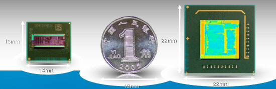
The Intel Atom processor (left) vs. The Poulsbo chipset (right)
With Poulsbo being a 130nm part, it also helps explain why Atom is reserved for larger-than-iPhone devices today: the pair of chips simply wouldn't fit in anything too small. There are obvious power consumption concerns as well, but physically getting these two into a smartphone-sized device is going to be impossible until the next iteration.
At a high level, Poulsbo looks to be no different than your run of the mill Intel chipset with integrated graphics:
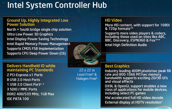
You'll quickly notice that the single chip solution, what Intel is calling a System Controller Hub (SCH) is a bit more unique. Instead of re-using a desktop chipset, Intel architected Poulsbo from scratch. In order to conserve power things like SATA and some of the USB ports were ripped out of the design. The designers chose to move back to PATA mostly because of power and smaller drives. Apparently in an idle state there isn't a power difference between PATA and SATA, but when actively transferring data SATA consumes much higher power due to its serial nature.
The FSB and memory frequencies are locked together which reduces power and PLL count. The chipset features a single channel DDR2-400/533 memory controller.
Poulsbo supports HD audio (Azalia, not the HD audio codecs) but reduced the number of audio engines supported in order to keep power under control. Only 2 channel audio is supported but you can access the audio interface externally, so conceivably you could dock an Atom device (such as a MID) and using an external codec get full 7.1 support.
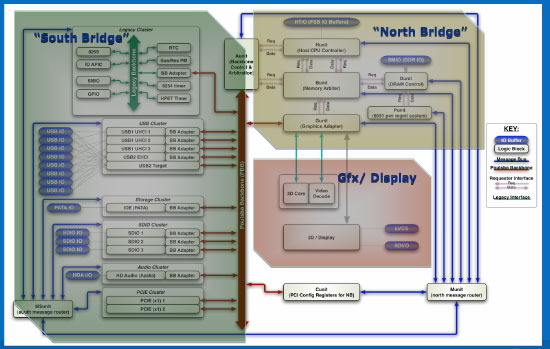
The parts of Poulsbo
Intel also developed a fairly sophisticated message fabric to send data across the SCH - think of it as an on-chip Ethernet network for carrying things like interrupts and power management signals across the chip in an efficient manner.
Poulsbo introduces a new FSB to memory bridge that's much simpler than conventional designs. In most chipsets you have many different queues for traffic between the FSB and memory subsystem designed to extract the best possible performance from the platform. With Poulsbo the designers simply outfitted the memory controller with a large 8K memory and all FSB/memory traffic must go through that. The single memory storage made validation a lot easier, the chipset itself a lot smaller but could incur a performance hit. The MCH/North Bridge part of the SCH is around 20% of the area of what traditional MCH/North Bridges are thanks to this approach.
The ICH/South Bridge parts of Poulsbo are similarly trimmed. Years of legacy have been stripped out of the chipset, there's no parallel port, no floppy disk controller. In mainstream chipsets as long as someone is using the feature, it must be kept in play - the same wasn't true for Poulsbo. If the target market didn't need it, the feature wasn't going in the chipset.
The benefit of cutting the fat in Poulsbo is that the chipset was physically smaller with fewer gates, meaning lower leakage power.
In a highly atypical move for Intel, Poulsbo also supports non-standard 1.5V DDR2 memory. There's no official JEDEC spec for 1.5V DDR2 memory but many vendors have good enough modules that will work at 1.5V, so if an OEM wants to undervolt its memory the chipset will support it.
Much of the Poulsbo's design couldn't have been done had it not been for the Atom project. There are many revolutionary techniques at work within Poulsbo, it's a more modular design, a more efficient design and potentially holds the key to better chipset design in general - but none of these techniques were ever allowed to surface before.
Intel's chipset business is like a clock, every year a new platform is expected and some of the more revolutionary changes that could potentially interrupt the normal flow of things are generally frowned upon. Poulsbo, at least internally, broke down a lot of these barriers. While it's far from the highest performance chipset Intel has ever produced, Poulsbo requires roughly half the power of mainstream chipsets. Intel has been on an efficiency kick with its CPUs for a few years now, Poulsbo may help ignite a similar trend with chipsets as well.


46 Comments
View All Comments
adntaylor - Tuesday, April 8, 2008 - link
On that chart with price / power, you need to be clearer...For price, you show the combined price for CPU + Chipset. For power, you say just the CPU... so 0.65W for the CPU... but you're conveniently ignoring the >2W figure for the chipset!!! This absolutely flatters Intel wherever possible.
AMD are just as misleading - they describe the Geode LX as "1W" which excludes the non-CPU core parts of the chip (which is an integrated CPU + GMCH)
Just please be honest - the figures are out there in the Intel datasheets... it takes 10 minutes to check.
Clauzii - Friday, April 4, 2008 - link
I still have a PowerVR 4MB addon card, runnung in tandem with a Rage128Pro. Quite a combination w. 15 FPS in Tombraider. Constant(!) 15FPS, that is..Amazing what they actually achieved back in 95!
Clauzii - Friday, April 4, 2008 - link
Ooops!Totally misplaced that. Sorry.
wimaxltepro - Friday, April 4, 2008 - link
The Atom represents a shift in processor architecture that is the most dramatic departure for Intel since introduction of x86 processors... the philosophy of how computing itself occurs from centralized processors to distributed processing based on an extension of the popular x86 instruction set.The Atom is not about the immediate prospects for the Atom or Nehalem products: we will likely see members of Intel's new product family be used in embedded applications in consumer products and in areas where specialized communications processors are more the rule. While not optimized for use in specific networking applications, the products capitalize on the wide range of support available in IT/Networking to develop common functions that leverage the low cost, low power/processing capability to be used as a common denominator for a wide range of applications.
Intel has been built on the 'Wintel' architecture: massively integrated chips needed to handle the massively integrated operating systems and applications of Windows (and Apple) environments. The Atom allows migration and broadening out from that architectural motif to a very highly distributed architecture. So, the increased parallelism found in the internal chip architecture is enabling of changes in external system architectures and device applications that go well beyond the typical domain of Intel.. and right into the domain of 'personal wireless broadband' and SDWN, Smart Distributed Wireless broadband Network.
The decisions about in-order vs. out of-order instruction streams, memory architecture, I/O architecture have been made in light of the broad vision for how computing, networking and, out of hand, how wireless enabled broadband networking including WiMAX will occur. This should be understood for what it represents as a shift in direction for Intel both in response to broad industry shifts and as a trend setting development.
jtleon - Friday, April 4, 2008 - link
Thanks to all the flash player ads, etc., a mobile web device will continuously avoid switching to low power states. Thus one could argue that advertising will be carbon footprint enemy of the internet's future. This is already becoming the case for desktop/laptop machines.Without such continuous (arguably wasted) consumption of CPU power, then Intel's engineered power management might have a significant impact on the value of the Atom.
Regards,
jtleon
0WaxMan0 - Friday, April 4, 2008 - link
I am definatly much impressed and enthused by intels work here, the future looks interesting esp for those of us who like low power cross compatible computing products.However I have to point out that a low power modern x86 cpu has allready been done infact 4 years ago with AMD's Geode. While technically much weaker than the Atom and with out any where near the scalability (single core design etc.) the Geode has been available in the same TDP ranges for a good long while. Take a look here http://www.amdboard.com/geode.html">http://www.amdboard.com/geode.html for some old stuff.
I do hope that the Intel name and hype makes more of an impact than AMD managed.
whycode - Thursday, April 3, 2008 - link
Does the TDP quoted include the chipset? Or is that CPU only?IntelUser2000 - Thursday, April 3, 2008 - link
Anand, the Pentium M does not feature Macro Ops Fusion. Its Core 2 Duo that started Macro Ops Fusion.Anand Lal Shimpi - Thursday, April 3, 2008 - link
You're correct, I was referencing micro-op fusion. I've made the appropriate correction :)Take care,
Anand
squito - Wednesday, April 2, 2008 - link
Am I the only one shocked to see that Poulsbo is a 130nm part...