Intel's Decision
Instead of allowing AMD and Cyrix to gobble up any more of Intel's market share, Intel chose option number 2, and found a way around the problems they had with the Pentium Pro, the Pentium II's Single Edge Contact Connector. By moving the L2 cache off the motherboard, and onto a processor card, the cache could be run at a much higher frequency (in the case of the Pentium II, 1/2 the clock speed of the CPU), while at the same time the overall cost of the processor would remain reasonable, and the limitations of the Socket-7 standard would be avoided completely.
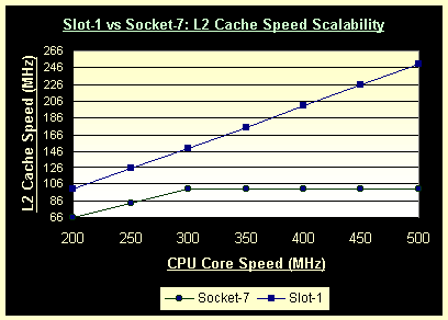
As Intel, AMD, and Cyrix all quickly noticed (along with their users), the performance benefit we were receiving from increased clock frequencies (i.e. a Pentium MMX 233 vs a Pentium MMX 200) was decreasing with every jump in clock speed. The reason being as alluded to before, that the speed of the L2 cache on Socket-7 systems wasn't proportionally increasing in comparison to the CPU's clock speed. With the Slot-1 interface of the Pentium II leaving enough room for an external L2 cache, running at 1/2 clock speed, to be placed on the processor card, Intel succeeded in distancing themselves from the rest of the competition and at the same time they succeeded in developing a technology that would remain Intel-only until they decided otherwise.
Driving Costs Lower
That performance advantage, high-speed L2 cache, and larger packaging made the cost of Intel's Pentium II a bit higher than most felt like paying, and after a quick look at the latest polls at the time, it was obvious that Intel needed to be able to compete with AMD and Cyrix on the cost-efficient end of things as well. Intel decided that the best way to do such a thing would be to take that precious L2 cache off the processor card, and sell a lower cost Pentium II that would eventually replace the Pentium MMX at the low end of the performance spectrum. Intel called this release, the Celeron processor, unfortunately, for Intel's sake, the Celeron did little more than get horrible press from most publications, and had it not been for its incredible gaming performance as an overclocked chip, the Celeron would have been a complete failure.
It has been said that history often repeats itself, however in this case, Intel corrected the original problems they had with the Pentium Pro and decided to give integrated L2 cache another try. This time Intel attempted to integrate the L2 cache onto the die of the chip itself, since the 0.25 micron manufacturing process of the current Intel line of processors allowed for much more to be integrated into a much smaller area, Intel's next concoction was an instant hit, in both price and performance respects. The Celeron A was born, featuring a full 128KB of L2 cache running at clock speed, and a price that undermined virtually all of the competition, sometimes including Intel's own products as well.
The high yields of the Celeron A made it one of Intel's definite successes, however at its release the Pentium II had already matured to the point where a high quality Intel processor wasn't something to brag about. Intel was wrong in assuming that placing the cache in an external package outside of the CPU would be the best option for them as a CPU manufacturer, however were they wrong about making the journey to the slot as well?
Apparently they were, and as a shocking yet expected news release, Intel finally announced that they would be moving back to a socket interface for their newer Celeron CPUs to lower costs. If you think about it, with the Celeron, there is really no reason for the processor card, since everything is located on the processor itself, so it would make sense to get rid of the card and simply plug the processor into a motherboard….and that's exactly what Intel did.


0 Comments
View All Comments