Intel Demonstrates new 45nm Transistors and Conroe's Successor
by Anand Lal Shimpi on January 27, 2007 12:00 AM EST- Posted in
- CPUs
More Efficient Transistors
The basic function of a transistor as found in modern day microprocessors is to act as a switch with two states: on and off. When the transistor is on, current is allowed to flow from one terminal to the other (source to drain), and when it is off current shouldn't flow. Making enough current flow when it should and minimizing the amount that flows when it shouldn't is one of the major hurdles to making smaller transistors that run cooler/faster.
Below we have a typical CMOS transistor diagramed and labeled:
![]()
The voltage present at the Gate and the Source will determine whether or not current will flow in the transistor. Intel's 45nm process makes significant changes to two of the components in this transistor diagram: the gate electrode and the gate dielectric.
You can probably guess that as transistors get smaller, all of the parts of the transistor get smaller as well. The problem is that when some of these features get too small, they start behaving inappropriately. Case in point is the gate dielectric; with Intel's 90nm and 65nm processes, the gate dielectric was shrunk to a thickness of 1.2nm - the equivalent of about 5 atoms. The benefit of a very thin gate dielectric is that it increases the gate field effect, which increases drive current and reduces Source-drain leakage current. However, with such a thin gate dielectric electrons can tunnel directly through the layer and show up as leakage current - in other words, current would flow when it was not supposed to, translating into power wasted. On an individual transistor scale it's not such a big deal, but when you keep in mind that Penryn will have around 410 million of these transistors (820 million for quad-core) the leakage current/power draw does add up.
At 1.2nm, the gate oxide/gate dielectric in Intel's 90nm and 65nm transistors was as thin as Intel could make it without losing a great deal of power due to gate oxide leakage current. In order to make the move to 45nm Intel had to do something to thin the gate oxide without drastically increasing gate oxide leakage current.
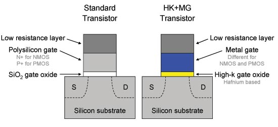
Intel solved the gate oxide leakage problem by replacing the SiO2 gate dielectric with a material that has a higher k-value, in this case a Hafnium based material. A high-k dielectric here actually increases drive current at the same thickness as the previous SiO2 dielectric, while reducing gate leakage as well. Intel isn't disclosing how thick the Hafnium gate dielectric layer is in its 45nm transistors, but we do know that it is thicker than the 1.2nm SiO2 gate dielectric used in previous 90nm and 65nm transistors.
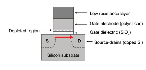
The second problem Intel is addressing with its 45nm transistors is a fundamental issue with the polysilicon gate electrode. The role of the gate electrode is important as it is what enables current to be driven through the transistor and as such it plays a role in how much current can be delivered. The polysilicon material that the gate electrode is made of has a tendency to form a region of depleted conducting carriers at the bottom of the gate, which reduces the drive strength of the transistor (less current flows when it needs to).
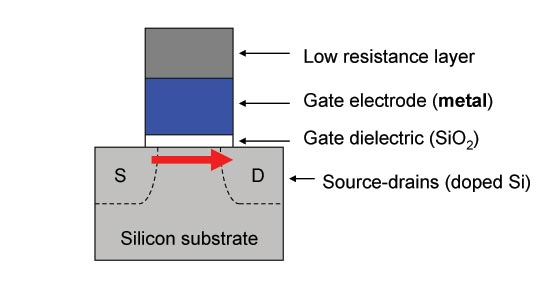
Intel's new 45nm transistors solve this problem by replacing the polysilicon gate electrode with a metal gate electrode, which completely eliminates the depleted region thus increasing the drive current.
Intel has been researching this High-k + Metal Gate (HK+MG) combination in transistors for a handful of years now, with hundreds of material options for metal gate electrodes and high-k dielectrics. The actual combination of high-k and metal gate material isn't being disclosed at this time, most likely to protect Intel's research and maintain the manufacturing advantage as long as possible. Intel expects that no other company will have HK+MG transistors until they reach 32nm or later.
The tangible advantages of these changes in materials in combination with the smaller 45nm process are quite large. According to Intel, the move from 65nm to 45nm yields a 30% reduction in transistor switching power because of the simple fact that smaller transistors have less parasitic capacitance and require less power to switch on and off.
Because of the combination of a high-k dielectric and the metal gate electrode, Intel is quoting a greater than 20% improvement in switching speed compared to its 65nm transistors. At the same speed as its 65nm transistors, there's a greater than 5x reduction in source-drain leakage power and a greater than 10x reduction in gate oxide leakage power; the latter is due entirely to the use of a high-k dielectric in the transistor. The end results of all of this are more power efficient processors, the first of which we should see by the end of this year.


59 Comments
View All Comments
quidpro - Monday, February 26, 2007 - link
What is Glaze? google is not helping.Hoser McMoose - Wednesday, January 31, 2007 - link
The calculation for the number of transistors for cache is off by a fairly significant amount in this article! The article states 288M transistors for 6MB of cache, which is FAR too low!Actual transistors for 6MB cache, if we assume ZERO redundancy is:
6MB * 1024KB/MB * 1024B/KB = 6,291,456 bytes
6,291,456 bytes * 9 bits/byte = 56,623,104 bits (remember ECC makes it 9 bits, not 8)
56,623,104 bits * 6 bits/transistor ~= 340M transistors
In reality it is actually probably more like 350 or 360M transistors required for 6MB of L2 cache since you always want a bit of redundancy. It's a bad thing if you have to throw out an entire chip due to a single bit error in your 6MB of cache!
Now, taking those numbers, if we assume that the 410M Transistor figure is accurate, the change in transistors from Conroe to Penryn is a bit different.
Conroe has 291M transistors of which at least 226M are L2 cache. That leaves only 65M assuming no redundancy, or maybe more like 50M transistors with a few redundant cache cells. According to www.sandpile.org (and I have no idea what their source is) each core of the Core 2 Duo has only 19M logic transistors. If this is accurate then it's actually HUGELY impressive, since that is WAY less then either the Pentium 4 or the Athlon64.
Murst - Monday, January 29, 2007 - link
"Intel isn't disclosing how thick the Hafnium gate dielectric layer is in its 45nm transistors, but we do know that it is thicker than the 1.2nm SiO2 gate dielectric used in previous 90nm and 65nm transistors."Why would intel make the gate larger in a shrink? Is this a typo, or is there some huge benefit to this?
IntelUser2000 - Tuesday, January 30, 2007 - link
The reason is that making the gate dielectric thinner than 1.2nm is not a good idea. 1.2nm dielectric is already equivalent to 5 atoms in thickness. Electrons can literally squeeze through the dielectric "insulator" because the dielectric is so thin. Because the material used for the dielectric layer is different from the 65nm generation, they can make the dielectric thicker without sacrificing speed characteristics. So they can increase speed AND have substantially less leakage.
Visual - Monday, January 29, 2007 - link
So, I'm a bit out of the loop lately, can anyone brief me up?Are there any new sockets, chipsets, ram changes or anything expected together with these new 45nm goodies? Or will I be fine getting a new system come Q2, and upgrading to Penryn when it's out and affordable?
ceefka - Monday, January 29, 2007 - link
I wonder if booting OXS with the new chip indicates that PC-users can soon use OSX too without having to buy a Mac. That would allow to mix and match a bit more with apps.Netopia - Sunday, January 28, 2007 - link
100 * 100 =10,000
50 * 50 = 2,500
That's a 4x improvement, not a 2x!
Joe
coldpower27 - Sunday, January 28, 2007 - link
That is not how it works...65 x 65 = 4225
45 x 45 = 2025
2025/4225 = 48% the size of the 65nm part, so close to 2x smaller.
IntelUser2000 - Sunday, January 28, 2007 - link
That's the theory. Intel's 45nm 6T SRAM size is 0.346um, and 65nm SRAM cell size is 0.57um. That's only 39% reduction(61% of the size). In addition, SRAM, which is used for cache, has the best potential for scaling. The cores will have likely worse scaling than 61%.
coldpower27 - Monday, January 29, 2007 - link
Yes, I was just presenting the mathematical example of the calculation, I wasn't going into having real world factors involved. Since in this article Anandtech simplified things with just the 2x smaller statement.