NVIDIA nForce4 SLI XE: Enthusiast Features on a Budget
by Gary Key on March 23, 2006 12:05 AM EST- Posted in
- Motherboards
ECS C19-A SLI: Features
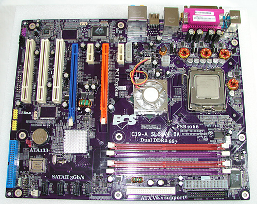
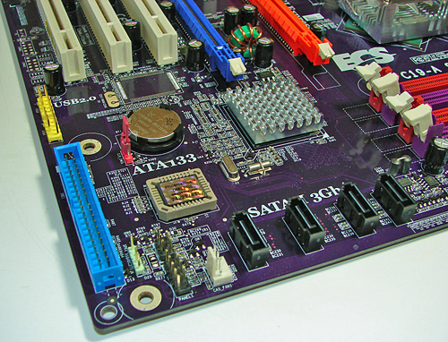
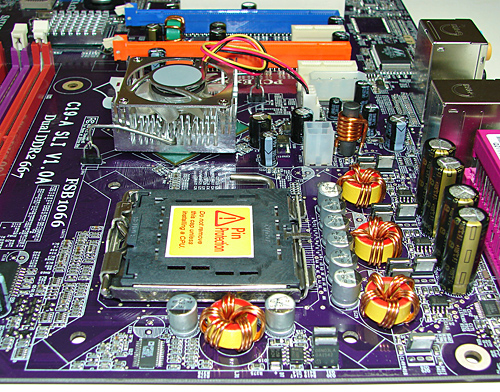
The blue primary NVIDIA nForce4 IDE port connector is located on the left edge of the board and did not present any connection issues in our mid-size ATX case. The location of this connector is very good for most cases and those users still utilizing IDE hard drives. The chassis panel and fan header is located between the primary IDE connector and the nForce4 SATA ports. The BIOS chip is located directly above the chassis panel and fan header.
The yellow NVIDIA nForce4 USB connectors are located above the primary IDE connector and along the edge of the board. The battery and CMOS jumper block is located above the BIOS and to the left of the MCP chipset. The clear CMOS jumper block is a traditional jumper design and is easily accessed.
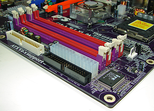
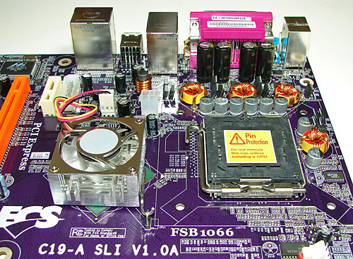
The first PCI Express x1 connector is located to the right of the 4-pin 12V connector. This 4-pin 12V connector is required for dual graphic card or SLI operation. The location of this PCI Express x1 connector allows installation of most peripheral PCI Express cards and is not blocked by most video card designs.
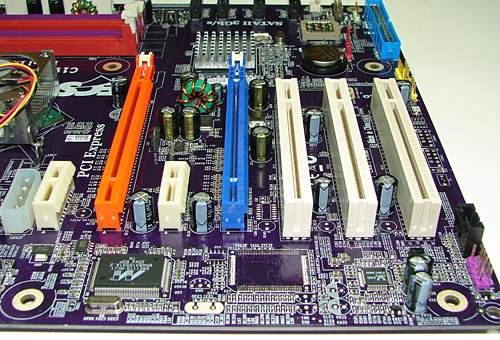
The first physical x16 connector (orange) is located next, followed by the second PCI Express x1 connector. When utilizing a dual slot video card, this PCI Express x1 connector will be physically rendered useless. We did not have any issues utilizing this slot with video cards containing single slot cooling systems.
The second physical x16 connector (blue) is located next, followed by the three PCI 2.3 compliant 32-bit connectors. When utilizing a dual slot video card, the first PCI connector will be rendered physically useless. There were no issues utilizing this slot with video cards containing single slot cooling systems.
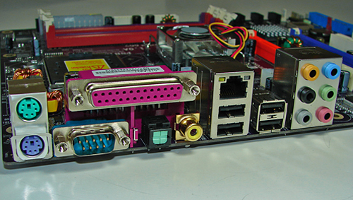
The Marvell 88E1115 Gigabit Ethernet LAN PHY is located in front of the first x16 connector. The Realtek ALC-883 HD audio codec is located in front of the number two PCI connector. The front panel audio header is color-coded purple and located at the edge of the board with the black analog audio input connector situated behind it.
The NVIDIA nForce4 SLI XE SPP chipset is actively cooled with a large heat sink/fan unit that did not interfere with any installed peripherals. Our only concern is the lifespan of the fan and it does generate a slight whirling sound during operation.
The blue primary NVIDIA nForce4 IDE port connector is located on the left edge of the board and did not present any connection issues in our mid-size ATX case. The location of this connector is very good for most cases and those users still utilizing IDE hard drives. The chassis panel and fan header is located between the primary IDE connector and the nForce4 SATA ports. The BIOS chip is located directly above the chassis panel and fan header.
The yellow NVIDIA nForce4 USB connectors are located above the primary IDE connector and along the edge of the board. The battery and CMOS jumper block is located above the BIOS and to the left of the MCP chipset. The clear CMOS jumper block is a traditional jumper design and is easily accessed.
The first PCI Express x1 connector is located to the right of the 4-pin 12V connector. This 4-pin 12V connector is required for dual graphic card or SLI operation. The location of this PCI Express x1 connector allows installation of most peripheral PCI Express cards and is not blocked by most video card designs.
The first physical x16 connector (orange) is located next, followed by the second PCI Express x1 connector. When utilizing a dual slot video card, this PCI Express x1 connector will be physically rendered useless. We did not have any issues utilizing this slot with video cards containing single slot cooling systems.
The second physical x16 connector (blue) is located next, followed by the three PCI 2.3 compliant 32-bit connectors. When utilizing a dual slot video card, the first PCI connector will be rendered physically useless. There were no issues utilizing this slot with video cards containing single slot cooling systems.
The Marvell 88E1115 Gigabit Ethernet LAN PHY is located in front of the first x16 connector. The Realtek ALC-883 HD audio codec is located in front of the number two PCI connector. The front panel audio header is color-coded purple and located at the edge of the board with the black analog audio input connector situated behind it.
The NVIDIA nForce4 SLI XE SPP chipset is actively cooled with a large heat sink/fan unit that did not interfere with any installed peripherals. Our only concern is the lifespan of the fan and it does generate a slight whirling sound during operation.


12 Comments
View All Comments
blackmetalegg - Friday, March 24, 2006 - link
"Unfortunately, we ran into an issue with this process as the clear CMOS process sometimes required the removal of the battery for the jumper process to work. This process is not acceptable, considering how well other BIOS recovery systems work."Sounds a lot like the reviewer is too lazy to use his finger to release the battery from its holder.
Gary Key - Friday, March 24, 2006 - link
Certainly not lazy as I removed the battery at least a dozen times during testing. The fact remains that having to remove the battery is not an acceptable option when the clear CMOS jumper does not work over 60% of the time because the bios self recovery routine fails 85% of the time when the memory settings are extended past the board's ability to boot properly. This only occurred a couple of times when setting the FSB past the board's limit.
kmmatney - Friday, March 24, 2006 - link
I hate removing the battery. I broke the flimsy battery clip off of one motherboard doing this, and had to solder new wires in place and dangle a new battery from it. Removing the battery for a BIOS clear is not good.cornfedone - Thursday, March 23, 2006 - link
Obviously this mobo wasn't tested before release or it wouldn't have all the problems it has.phillock - Thursday, February 1, 2018 - link
Sounds a lot like the reviewer is too lazy to use his finger to release the battery from its holder.https://jumjex.bandcamp.com/releases
Puddleglum - Thursday, March 23, 2006 - link
Not sure if it's worth fixing or not, but the Content Creation (Disk Controller Performance) chart shows the Biostar TForce4 in red, mistaken as the board being tested.smut - Thursday, March 23, 2006 - link
Is this going to be an Intel only board?Gary Key - Thursday, March 23, 2006 - link
Yes. The upcoming NVIDIA nForce 500 launch will address chipset updates to the AMD product family.
bldckstark - Thursday, March 23, 2006 - link
No, upon release the board will come with alternate CPU sockets included in the box. You got an AMD? Just pop out the Intel socket and plug in the AMD socket. Gat a VIA, Cyrix, or TI85 chip? Just break the chosen socket out of the plastic holders like a model car part.Oh, wait, I guess you want to know if ECS is going to make an AMD board. Duh.
Gary Key - Thursday, March 23, 2006 - link
Our next article will have a high resolution picture of the capacitors and other items of importance in a pop-up window. I am sure the capacitors utilized on this board will be of interest to you. ;->