FIRST LOOK: ULi M1697 for Athlon 64/x2
by Wesley Fink on December 13, 2005 12:05 AM EST- Posted in
- CPUs
Basic Features: ULi M1697 Single Chip
The ULi Award BIOS provides a typical range of BIOS control options for a Reference Board used to qualify a chipset. The wide 200 to 400 range for CPU clock was a pleasant surprise, but it is somewhat academic with no memory voltage controls present in the BIOS. The memory tweaking adjustments were extensive, but of limited use without some means of controlling memory voltage. Reference Boards demonstrate chipset features and capabilities to manufacturers, and ULi clearly shows that the M1697 is capable of supporting whatever range of BIOS control or Voltage control features that the manufacturer might wish to implement.
The location of the floppy connector at the bottom of the board will be a long reach for floppy users. Many buyers don’t care about floppies any more, but if you still use them, the bottom of the board is an inconvenient and hard to reach location.
| ULi M1697 | |
| CPU Interface | Socket 939 Athlon 64 |
| Chipset | ULi M1697 Single-Chip |
| Bus Speeds | 200 to 400MHz in 1MHz Increments |
| PCIe Speeds | 100-125MHz in 1MHz Increments |
| PCI/AGP | Fixed at 33/66 |
| AMD K8 Cool'n'Quiet | Auto, Disable |
| Core Voltage | Startup, 0.825V to 1.55V in 0.025V increments |
| CPU Clock Multiplier | Startup, 4x-25x in 1X increments |
| HyperTransport Frequency | 1000MHz (1GHz) |
| HyperTransport Multiplier | 200, 400, 600, 800, 1000, Auto |
| DRAM Voltage | Provision for 2.62V, 2.72V (Not implemented) |
| HyperTransport Voltage | 1.20, 1.25, 1.30, 1.35, 1.40V by DIP Switch |
| Chipset Voltage | 1.80 to 2.2V in .05V increments by DIP Switch |
| PCIe Voltage | 1.80 to 2.0V in .05V increments by DIP Switch |
| M1697 Resume Power | 1.70, 1.80, 1.85, 1.90, 2.02V by DIP Switch |
| Memory Slots | Four 184-pin DDR DIMM Slots Dual-Channel Configuration Regular Unbuffered Memory to 4GB Total |
| Expansion Slots | 1 PCIe x16 (or 2 PCIe x8) 1 x1 PCIe 1 x2 PCIe 1 x4 PCIe 3 PCI Slots 1 CNR Slot 1 LPC slot |
| Onboard SATA/RAID | 4 SATA2 3Gb/s Drives by ULi M1597 (RAID 0,1,0+1,5,JBOD) |
| Onboard IDE/IDE RAID | Two Standard ATA133/100/66 (4 drives) |
| Onboard USB 2.0/IEEE-1394 | 8 USB 2.0 ports supported by ULi M1597 No Firewire (Optional) |
| Onboard LAN | 10/100 Ethernet by Realtek PNY |
| Onboard Audio | HD Azalia 7.1 by Realtek ALC883 |
| BIOS Revision | Award OCAP1130 Evaluation ROM |
The ULi Award BIOS provides a typical range of BIOS control options for a Reference Board used to qualify a chipset. The wide 200 to 400 range for CPU clock was a pleasant surprise, but it is somewhat academic with no memory voltage controls present in the BIOS. The memory tweaking adjustments were extensive, but of limited use without some means of controlling memory voltage. Reference Boards demonstrate chipset features and capabilities to manufacturers, and ULi clearly shows that the M1697 is capable of supporting whatever range of BIOS control or Voltage control features that the manufacturer might wish to implement.
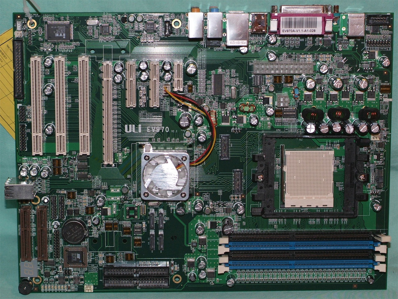
Click to enlarge.
The location of the floppy connector at the bottom of the board will be a long reach for floppy users. Many buyers don’t care about floppies any more, but if you still use them, the bottom of the board is an inconvenient and hard to reach location.


51 Comments
View All Comments
Scarceas - Thursday, December 15, 2005 - link
I presumed that ULI provided Anandtech with the sample to review... if you think about it, there are some wierd angles on that... A big deal like that isn't hammered out in a couple of days. ULI "brass" knew the sale was coming.It's kind of wierd, IMO, to send out stuff for reviews as you're going under.
I suspect that nVidia will sit on any tech they acquire, and not implement it. I was sorely disappointed that they sat on the GigaPixel technology a few years back, and there was of course more from the 3dfx acquisition that they never implemented.
IRQ Conflict - Wednesday, December 14, 2005 - link
Too bad this chipset is doomed before it even gets implemented LOL!http://www.nvidia.com/object/IO_28250.html">LinkPuddleglum - Wednesday, December 14, 2005 - link
https://www.nvidia.com/object/IO_28250.html">https://www.nvidia.com/object/IO_28250.htmlTorched - Wednesday, December 14, 2005 - link
Bad link on above post. You can read about Nvidia buying out ULi http://www.theinquirer.net/?article=28333">hereIRQ Conflict - Wednesday, December 14, 2005 - link
wierd, it was working yesterday? Oh well nVidia's following M$'s lead again. I can still smell the embers of the 3dfx acquasition.Peter - Tuesday, December 13, 2005 - link
And yet again, we're seeing Anandtech experts (?) evaluate the RAM controller properties of an AMD64 chipset.Hello?
The RAM controller is in the CPU, folks. Time to acknowledge that and skip that step in a chipset review.
Puddleglum - Wednesday, December 14, 2005 - link
Peter, this is what you were referencing:I don't see the words "controller" or "chipset" in there, and yet you say that the article evaluates the RAM controller properties of the chipsets. What he said about the lack of memory voltage adjustments was not referencing the chipset, but the method that Anandtech uses to overclock their boards.How did you come to think that the article mentioned the RAM controller?
Peter - Thursday, December 15, 2005 - link
I'm referring to the following statements on page 4:>Memory Stress Testing: Since this is a new chipset, the best setting for tRAS was first determined.
>This means that any setting from 6 to 11 tRAS will work well with this chipset.
>*7T was determined by MemTest86 benchmarks to deliver the widest bandwidth with the ULi M1697 chipset.
For anyone who's looked at the block diagram on page 2, it should be bleeding obvious that the RAM isn't the chipset's business at all.
Cygni - Tuesday, December 13, 2005 - link
Uhhhhh... havent used many A64 boards lately? ;) The ability to run low latency timings is very highly regulated by the board and chipset. You cant just drop any stick of ram in any board and get identical timings.The memory controller may be on the chip itself, but this doesnt eliminate the board and chipset from the equation whatsoever.
Peter - Wednesday, December 14, 2005 - link
AMD64 architecture totally eliminates the chipset from anything that is even remotely to do with the RAM bus. That's the point, and you're not getting it either.