NV45's on Package PCIe to AGP HSI
Our discussion brings us to the conclusion that an external bridge is not going to incur a tangible performance hit, but it may cause headaches and added cost on the OEM's side due to complications with additional component layout and parallel bus routing (which certainly complicates pricing and profitability). And the solution is to move the bridge off of the card and onto the GPU package.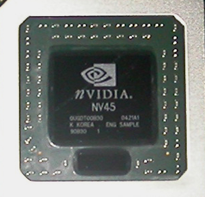
The tiny rectangle underneath the GPU is the HSI.
Now, not only is the HSI out of the vendors' hair, but it will also be cooled by the same HSF that sits on the GPU. This GPU looks and feels like a native solution to vendors (and by our benchmarks, it even acts very much like a native solution).
Dropping this thing on the package may seem out of left field, but even Intel has gone the additional-component-on-package route in the past; the original Pentium Pro had on package cache. A precedent like this begs the question: why didn't anyone think of this in the first place? This really makes perfect sense, especially if rumors are true that it's difficult to get a hold of HSI components unless bundled with a GPU.
So what's the down side? Well, there's still the issue of having less than PCIe bandwidth. This isn't going to be an issue for games in their current state, and won't likely be an real bottleneck in the future. Even on AGP, framebuffer read speed was only a couple of hundred MB/s on NVIDIA cards (and even less on ATI). The ability to get good traffic back over the bus has more to do with the GPU than the availability of bandwidth at this point.
The real thing that NVIDIA loses out on with a bridge is the ability to run multiple video streams up and down the PCIe bus with as much theoretical ease as ATI has. We are working hard to come up with some up and downstream PCIe benchmarks that will tell the real story about what is possible with framebuffer reads, and what is possible with video I/O on native and bridged PCIe GPUs.
But for now, we have NV45. No tangible performance impact under current games due to bridging (though a few odd numbers here and there with our current beta drivers), and now no added headache or extra development cost to OEMs over the ATI solution. With all that cleared up, let's head on to the tests.


14 Comments
View All Comments
Pete - Thursday, July 1, 2004 - link
Thanks much for the prompt reply, Derek.DerekWilson - Wednesday, June 30, 2004 - link
PPro cahce was a seperate hunk of silicon nudged right up next to the core ;-) search google images for pentium pro and you'll see the what it looked like under there.Pete,
#1 not sure when that's going to happen, but it will be enevitable for both companies. How we get there is the question. ;-)
#2 our demo is the same, only drivers have changed from our previous tests. We are looking into IQ also...
hope that helps,
Derek Wilson
Pete - Tuesday, June 29, 2004 - link
Sorry, Derek, please ignore #3. For some reason I missed that you specified the 6800U (PCIe) was a custom-clocked NV45.Pete - Tuesday, June 29, 2004 - link
Hi Derek,Can you help clarify three things?
1. I remember reading that ATi would eventually move to all-PEG-native GPUs, and then use a bridge for AGP cards, similar to nV's future plans. Did you hear anything about this from ATi or their OEMs/partners?
2. Did you change your Far Cry demo, or are new drivers responsible for the impressive gains the 6800U has made to significantly overtake the X800XT(PE)?
3. The "NV45" in your charts is simply a higher-clocked "6800U (PCIe)," right? Did you down-clock the NV45 to attain the 6800U PCIe numbers used in Anand's earlier LGA article?
KF - Monday, June 28, 2004 - link
I'm not sure how garbled a recollecton can be, Minotaar. That's not the way I remember it. The PPro had the cache on separate chips in a complex package that plugged into a socket. PIIs, slot cartridge style, had separate cache chips at first, and no cache chips for the first Celeron, true. Later PIIs, and PII style Celerons had on-die full speed cache. On die, reduced size, cache for such as the notable 300 MHz (not 266) Celery that OCed 1.5x by setting the bus speed to 100 instead of 66.Back to the subject, There are some very odd results for a solution that is supposed to be, and mostly is, equal between AGP and PCIe.
GTMan32 - Monday, June 28, 2004 - link
There was a web site reporting that NVIDIA opened up one of ATIs PCIe chips and found it wasn't native but just had the bridging on-chip like the NV45.Then there was another comment that the ATI PCIe chips were clocked lower because of OEM fears that they were running too hot at the same speed as the AGP parts.
One could conclude that the tacked on AGP->PCIe bridge was causing this since it would be the same size as the AGP plus the extra circuits for the bridge. If the ATI solution was really native then it shouldn't have any heating problems?
But was all this just a rumor. I haven't heard anything on this since.
OCedHrt - Monday, June 28, 2004 - link
A possible explanation for the drop in performance on the PCIe cards could be due to specific optimizations that aren't enabled for the PCIe cards in the current drivers. Just a wild guess.ZobarStyl - Monday, June 28, 2004 - link
This bridging seems to be the perfect solution for first generation PCI-E chips which have nothing to gain over AGP anyway...just so long as nV doesn't get lazy and has a native PCI-E card by next gen (which might actually use the bandwidth), they really haven't lost anything with this solution. Good article.Filibuster - Monday, June 28, 2004 - link
Minotaar,The Pentium Pro, by todays standards, *does* have on package cache because it was not part of the cpu core. It is full cpu speed however.
http://members.iweb.net.au/~pstorr/pcbook/images/p...
The big deal about the Pentium 2 cache was that Intel had to make it that way so they could test the cache chips separately from the cpu and thus save money, because the PPRo was soo expensive.
Wonga - Monday, June 28, 2004 - link
-----Pentium Pro also had the advantage of clock speed cache, whereas P2's cache was bus speed.
-----
Well, if we want to be correct about everything, the P2's cache was not run at bus speed, but instead a fraction of the core speed. Half the core speed, to be precise.
Anyway, cheers for the review. Looks like nVidia listened to their OEM partners here and did the sensible thing bringing the HSI on package.