New ATI Products Confirmed: The X Series Line-up
by Derek Wilson on June 1, 2004 6:00 AM EST- Posted in
- GPUs
X800 PCI Express and X600
The only difference that we know about between R420 and R423 at this point is in the bus interface, but it is still possible that ATI will decide to increase the stock clock speed for their PCI Express parts to offer a little more incentive for enthusiasts to upgrade their systems. We do expect to see a Pro and an XT part much the same as the AGP line of cards.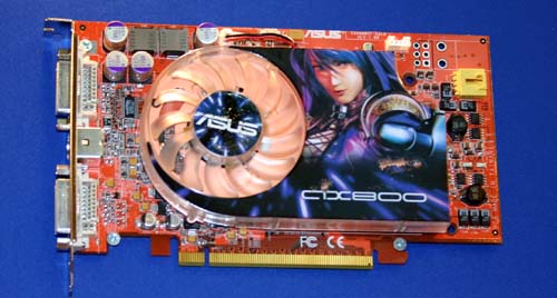
There will be two flavors of the X600 (Pro and XT), and this time around, the X600 Pro will be a PCI Express version of the 9600 Pro with 400MHz core and 300MHz (600MHz data rate) memory clocks. The X600 XT increases the memory speed to a 740MHz data rate, but the core clock remains the same at 500MHz. As such, we shouldn't expect to see much of a performance boost over current 9600 parts. This part is being marketed as the "world's first native PCI Express graphics card", but we'll have to wait for performance numbers to see if that really means anything.
Really, there isn't too much to say about these parts, since the only real difference is the bus interface. Of course, that doesn't mean that we don't have anything interesting to talk about, such as ATI's angle of attack on smaller fab processes.


10 Comments
View All Comments
Pumpkinierre - Tuesday, June 1, 2004 - link
Maybe 110nm is just on that limit where present technology allows the usual shrink/power reduction effect to be maintained without all the 90nm problems that really require a rethink to sort out. If that's the case it might be a good overclocker but could suffer from overvoltage or early death.quanta - Tuesday, June 1, 2004 - link
I wonder if anyone even cares about the 130nm X600 part, when they can just overclock 110nm X300 cards. But then again, die shrinks from 130nm to 90nm has given Intel a lot of trouble in the form of voltage leak and heat, I suspect X300 may not be able to run as fast as X600 without generate a lot more heat.Gholam - Tuesday, June 1, 2004 - link
Hmm, do I get it right that there won't be an 8-pipeline PCI-E Radeon? Straight from 4-pipeline X600 to 12-pipeline X800 PRO? Sounds somewhat strange... X800SE anyone?sxr7171 - Tuesday, June 1, 2004 - link
nserra - Tuesday, June 1, 2004 - link
#jcromanoNice explanation, have you used on processors too, like it would be amd 90nm athlon 64 die size?
This is much like digital camera 3mp to 5mp, it's almost the double but if you look at it, you would say it's only 30%/40% bigger. Or ati 160m transitors vs nvidia 222m. Ati is almost "big" but it has less 62m or a radeon 9600 less, funny isn't it?
Cycophant - Tuesday, June 1, 2004 - link
Small spelling mistake on the article intro:"Today, ATI fills out their new X series with three new PCI Express parts based on current __technolgoy__ that we are seeing. "
spikemike - Tuesday, June 1, 2004 - link
I don't believe blacks will look any blacker, you have to remember that the backlight is constant throughout the entire lcd. You can't control the brightness at a single pixel, so if you wanted to make blacks blacker then the whole screen would get darker, making the whites darker too, and in a very low darkness scene, you don't want to lose the black level resolution.vedin - Tuesday, June 1, 2004 - link
Darn..and I was really hoping that the X600 would be a little faster in the core and memory than the 9600XT. Say..550mhz? Honestly, I was hoping for a scaled down X800..so much for wishful thinking.jcromano - Tuesday, June 1, 2004 - link
I believe your claim that "a straight die shrink only accounts for about a 30% increase in space efficiency," found in paragraph 3 of the page titled "X300 Debuts at 110nm," may be in error.I'm not really sure what "space efficiency" is, but you make this claim in contrast to ATI's claim of a 40% increase in transistors per given area.
Assuming that the number of transistors per unit area scales inversely with the square of the (linear) process size, we have:
transistor density = k/d^2
For the old 130nm process, then,
transistor density (old value) = k/130^2.
For the new 110nm process,
transistor density (new value) = k/110^2.
The generally accepted way of presenting a percent increase or decrease is to use the old value as the denominator of the fraction. A formula such as this one would be appropriate:
(new value/old value) - 1
where the result is re-expressed as a percent, and a positive result is interpreted as an increase.
If we plug in, using k/110^2 for the new value (numerator) and k/130^2 for the old value (denominator), and cancel the k's, we get
130^2/110^2 - 1 = .39669 = 39.669%, which is admittedly lower than the 40% claimed by ATI, but close enough for me.
ducsauce - Tuesday, June 1, 2004 - link
I wonder if ATI will put out an All-in-wonder version of the x800 some time this year. The AIW 9800 pro is not going to keep up for long.